Prop Sigma Delta Theory
in Propeller 1
Hey all,
Today I messed around with building the ADC described in AN008. Despite reading everywhere that it wouldn't work on a breadboard, I figured I'd be stubborn and try it anyway. I got it working fairly well by oversampling at 12 bits and reading off the top 10. The key difference between the given design and mine is that I used 51K resistors and no caps. I got decent results, plots of scaled input voltage and measured values and error are below. While I wouldn't use it for reading precise sensors, something like potentiometers and other basic analog inputs would work great.
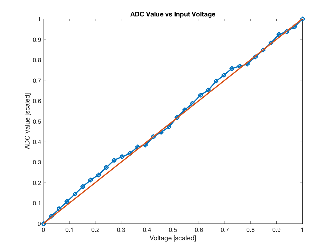
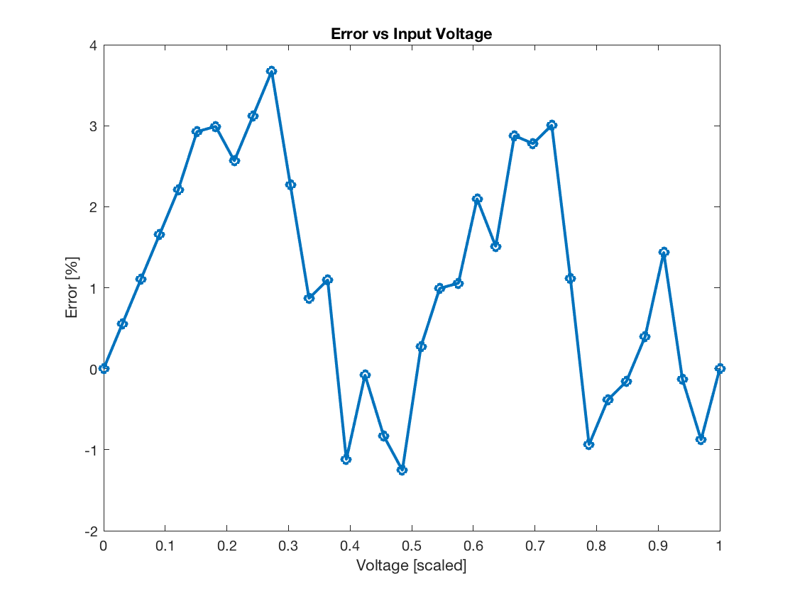
My main question is this: is there any analysis available describing the details of the design in AN008 and choice of capacitor/resistor values? For the capacitor/resistor to behave like an integrator, the RC constant must be large. But I found that the larger the capacitance, the larger the peak-peak voltage on the summing node, which we want to remain constant at Vdd/2. With no capacitance, it would remain very steadily around Vdd/2, while with a 1nF the circuit would not function at all (as described for breadboard designs). Surely the capacitance of the breadboard isn't enough to make the RC large, right? Why did removing the caps work?
I have a good understanding of circuits, feel free to give complicated answers
Nikita
Today I messed around with building the ADC described in AN008. Despite reading everywhere that it wouldn't work on a breadboard, I figured I'd be stubborn and try it anyway. I got it working fairly well by oversampling at 12 bits and reading off the top 10. The key difference between the given design and mine is that I used 51K resistors and no caps. I got decent results, plots of scaled input voltage and measured values and error are below. While I wouldn't use it for reading precise sensors, something like potentiometers and other basic analog inputs would work great.


My main question is this: is there any analysis available describing the details of the design in AN008 and choice of capacitor/resistor values? For the capacitor/resistor to behave like an integrator, the RC constant must be large. But I found that the larger the capacitance, the larger the peak-peak voltage on the summing node, which we want to remain constant at Vdd/2. With no capacitance, it would remain very steadily around Vdd/2, while with a 1nF the circuit would not function at all (as described for breadboard designs). Surely the capacitance of the breadboard isn't enough to make the RC large, right? Why did removing the caps work?
I have a good understanding of circuits, feel free to give complicated answers
Nikita


Comments
Certainly, it needs to be above some minimum value, in order to remember the residual voltage across many clock samples.
That does not really make sense.
SOME C must always be present.
With very low CAP values, the 'work' becomes relative. The output changes, but the error deviations are not good.
Some rough calcs : - Tau to Sysclk ratios.
10p*51k/(1/80M) = 40.8
20p*51k/(1/80M) = 81.6
33p*(51k/2)/(1/80M) = 67.32
If you want a 1% LSB, you need the cap to 'remember' averages over 100 sysclks. 0.1% needs 1000 sysclks, etc.
The Prop ADC uses the CMOS threshold as one reference, so it is prone to Vcc noise. Very large values of cap should continue to 'work' but with these, the supply noise can exceed the previous charge balance voltages.
(this also means some pins will be slightly better than others)
I would expect Prop ADC to follow a bathtub curve : less ENOB and worse linearity at very low and very high C's and some broadish band of R.C that gives best ENOB.
I'm curious how the circuit is laid out. Just to say "breadboard" leaves a lot to the imagination. Please fill in the picture or post a photo.
You've made interesting observations and have nice results. As jmg has said, in some ways it just doesn't make sense. On the other hand, breadboards can have hundreds of pF of stray capacitance to a ground plane and between tracks, so a lot of strange stuff could happen.
How does the tau required relate to the system clock and number of bits sampled? Do we want the RC charging to settle before the next clock? And, what are we calling "remembering"? From above, after Tau clock cycles, the value would have dropped by 37%, which isn't really "remembering".
I will play around with better Vdd decoupling, it's possible that with a 100pF, I'm already starting to see Vcc noise coupling in.
I agree that it doesn't make sense that it works without any caps.
I don't have the breadboard available, but here's a quick diagram attached. It shows the locations of the caps when installed. This breadboard is small, no power/ground tracks, just the standard 5-pin rows. All the leads were trimmed to install the components against the breadboard to reduce distances.
http://forums.parallax.com/discussion/97510/troubles-with-sigma-delta-adc/p1
http://forums.parallax.com/discussion/141965/high-precision-propeller-sigma-delta-adc/p1
http://forums.parallax.com/discussion/92201/adc-on-high-voltages
A classic/purist SDM uses a true integrator on the charge balancing, which means a 1% offset in voltage, will create a 1:99 sawtooth on the cap.
Small offsets generate lower frequency balance waveforms, and it is those lower frequencies you want to 'remember' to get higher bits on any ADC.
True, but those numbers give you a feel for the effects. Your plots show errors of 3~4%, which are one part in 25, and I would call high for any SDM.
You should be able to do better - I recall numbers like 10-12bits being mentioned for Prop ADCs ? ie under 0.1% errors.
High stability / Low Noise regulators should also give better results.
eg I'm curious about the new generation of low end regulators like
LDL1117S33R from ST - now stocked, and is simple, low cost and has good specs/$. 1A+, SOT223, 250uA typ IQ and 87dB 120Hz PSRR, and 60ppm noise
similar is
LDK320ADU33R - SOT89, 200mA, lower IQ of 60uA and comes in a 0.5% version (same PSRR, noise as LDL1117S33R)
Another way to improve AC mains rejection, is to have measurement times set to be whole-AC cycle multiples. Any coupled AC then averages to 0V.
Definitely no argument there, but I would expect to see results track theory to some extent here, not move in the opposite direction, at least with order of magnitude changes. The fact that I see Vpp of the input increase with capacitance is odd and I'm trying to understand why that might be.
The slower voltage changes with more capacitance likely make the circuit more susceptible to noise and hysteresis issues. I'm not aware of any studies into the hysteresis of the Propeller inputs. You might find interesting insights from measuring the frequency instead of duty cycle.
What is your voltage source?
I'm using a digital bench-top power supply, so very stable down to 1mV. I even connected through 10K to see how source resistance affects the system. Result: it doesn't really (aside from difference in gain).
Tomorrow I'll grab some scope captures and post them, maybe they will provide more insight.
How exactly are you measuring that ? I'd suspect your measuring / test setups are not quite ideal.
I measure it close to Propeller's pin with a scope, using a short ground connection for the reference lead.
Nice links, the second one mentions some ENOB values....
'(right now I get ~14-bits stable and ~16-bits rms with 2^18 clock cycles accumulated. at 5MHz)'
'.... I've slowed my code down to 5MHz (to save power) but still sample at 19Hz. The data so far looks like I'm getting 14 stable bits. So 1/16th the sample rate, and the noise is the same or better."
'Another note. Turning on the PLL and running with a 10MHz clock and 19Hz sample rate has 1.5-2x the noise of running without the PLL at 5MHz. This would indicate that using a fast crystal and no PLL is best for sigma delta precision.'
Suggests there may be some 'ideal MHz' from a best ADC viewpoint ? - as with most MCUs ADCs, you can clock higher, but after some point, the performance declines.
With the supplies as part of the reference in P1, digital noise is going to matter. Not sure if a crystal, or external clock is better ?
Has anyone tried ADC ENOB tests on the new FLiP (with new low-RFI (slower edges) clock?) - FLiP has SMPS and external clock, so is 'different' from older Prop layouts.
Rigol DS1104B (100 MHz) with RP2200 passive probes (150 MHz)
When I say "without caps" I mean without explicit values on the order of 1nf, and only the stray capacitances. I'll try to dig more and understand whats going on and why I see worse performance when adding explicit caps.
The clue may be in your first post...
I'd say 'wouldn't work' here is shorthand for 'will somewhat 'work', but at reduced performance levels, including artifacts...'
If I was testing this, I'd strive to have the Digital feedback pin (ADCout) drive the smallest possible load (aka very short track, just to Rfb), and look to have lowest noise on ADCin pin.
On ADCin, maybe pins P7 or P8 are better than P23, P24 ? ADCout may work better not too close to ADCin (ie at least one pin separated)
Less a plug-in breadboard and more a 3D/Manhattan test construction...
But, more to the point, if you're operating with a breadboard, without SMD components mounted near the Prop's pins, you might be getting the best that could be expected.
-Phil
So it seems that I can't get more than about 5 bits of accuracy anyway. I'll totally believe that given that I'm building this on a breadboard. Can you guys please provide some explanation as to what effects the breadboard imparts on the circuit to cause this loss of resolution?
Additionally, lets say I design a good PCB layout for this, what is the relationship between the RC constant and ENOB, assuming there are very low parasitics.
Charge sum sense, assumes the voltage on the CAP, is the averaged feedback voltage, and that is compared with the CMOS pin threshold ( ~ 50%).
- add in some spikes, and the decisions about go-up / go-down can go awol.
It only needs ~ 50mV of uncertainty, to drop you down to 5 bits of ADC.
See the other threads, where as good as 14 bits is reported, with some care on clocking MHz, (slower was better) as well as layout. 12b is more typical.
As ENOB climbs, other parts of the circuit start to need attention - supply noise of just 63uV, is equivalent to just over 15 bits.
Some ideas for improved testing could include running a second counter that inverts !A pin. That will be one sysclk delayed, but should track the voltage in pin.
With matched precision resistors, a RC filtered Mirror_!A, should give (exactly) the same DC voltage as Vin, and a merged !A,Mirror_!A RC node should average to the threshold voltage.
In both these test points, you look for change as you sweep, so they are quick to check.
In order of potential importance, I'd put L1 at the top. It is the inductance in the path from FB output pin on the Prop over to the breadboard. There is also inductance L2 back to the IN sense pin on the Prop, which wouldn't be so important (less current), except that there are also parasitic capacitances between your pins P25 and P26, and other parasitics possibly depending on the carrier board you have for your propeller. So L1, L2, C1 and C2 sort of lump together all the stuff that lies on the signal path between P25, P26 and the breadboard.
There is capacitance between tracks on the plugboard, for example, C3 would be a capacitance of about 100pF coupling the 3 volt transitions on the FB pin directly into the analog input. Hmmm.
Oh, and even if you remove your intentional capacitors to Vss and Vdd, you still have significant capacitance there in the form of C4 and C5, but not quite symmetric in relation to the summing node.
I've left off a lot of parasitic capacitors, for example, your feedback resistor Rf (51kΩ) is separated by 3 tracks that are floating and thus make a series combination of about 33pF in parallel with Rf. It is possible to shield nodes by connecting intervening tracks to ground, but then you have a capacitance to ground to consider.
I've also thrown in RL?, which is possible inductance of the resistors Rf and Ri. Are their leads cut as short as possible? Also the power supply leads add significant inductance in series with the capacitors. Not to mention again possible effects of power supply noise .
Pretty hard to analyze! (BTW, my 100pF figure for intertrack capacitance is a hazy memory, a guess, your milage may vary!)
consider the time it takes to acquire the desired number of bits. For example, it takes a minimum of 4096 clock to acquire 12 bits, and at 80MHz clkfreq that is 4096/80E6 = 51.2 microseconds. So with Rin=Rf=100kΩ (50kΩ equiv.), you'd need at least a 1nF capacitor.
I'm reasoning as follows. On the average, the extreme values you want to achieve, 1 and 4095, require that the feedback output stay in one state (high or low) 4095 out of 4096 cycles, then one cycle in the opposite state. The 4095 cycles are in theory very small triangular fluctuations and the one cycle that resets the process is one large transition. This last one is due to the extreme value of the voltage or current present at the input, in comparison to the small quantum of charge that is pumped in by each cycle of feedback.
Attached is a 'scope shot of a sigma-delta operating at a leisurely 20kHz RCSLOW with a 10nF capacitor, and 75kΩ equiv resistance. The point is that you can see the smaller transitions followed by a larger transition that resets the process. I wouldn't expect this setup to be capable of many bits, because the RC time constant (75E3Ω *10E-9F = 750 µS) is not even 8 times the clock period of 50µs. The swings are quite large, so noise and dither is less evident than when the process operates close to the threshold.
Thank you, that's all extremely useful information, and I'm starting to gain an intuition for what's going on! To answer your question, yes, the leads are all cut as short as possible and I'm using a quickstart board, so not great for added parasitics. But, I can easily see the parasitic Ls and Cs adding 50mv of unwanted spikes (I'm avoiding saying noise as that's a different can of worms here) to the feedback (and coupling into the analog input as well), so to jmg's point, I'm pretty much getting the best I can out of this system (5 bits).
So, ignoring C4 and C5, it seems like adding my capacitors causes the LC created by L2 and my caps to add voltage spikes to my summing node and actually reducing my resulting ENOB. Does that seem reasonable?
The QS has SMD pads for one channel of ADC, the other thread linked above suggests to cut the traces on those pins that go to the IO connector, to keep things compact.
The Power decoupling on the QS is not as good as it could have been, with longer, less direct PWR-CAP-GND paths.
There should be ENOB numbers about for that QS ADC, as it is a known reference point, widely used.
The Prop samples the sense input just before the transitions, and if the input is high, the feedback output transitions to low. And vice versa, input low, output transitions to high. The long drops come when the sense input is still high even though it already has had one period of drop.
For higher resolution, these periods have to be quite long, like 4096 clock periods for 12 bits, and the sense input has to stick well within a millivolt of the threshold. At the center of the range, the feedback frequency is high, like 40MHz for an 80MHz clock. That frequency does not require much filtering, but the fact remains that the entire cycle needs a full complement of clock cycles in order to resolve to 12 bits. The effect of noise or dither is to add or subtract transitions from the theoretical norm, and that then in order to maintain resolution necessitates sample averaging or acquisition over a longer period. It should all average out over the long term in order to meet the feedback restraint. However there are likely 1/f noise components, hard to remove.