Custom Layout Mods
 cgracey
Posts: 14,303
in Propeller 2
Over the last several days, I've been going over the layout, finding things that need sprucing up.
I think I'm done now, and Treehouse will be done making these edits tomorrow. Then, I'll get a new .gds file to review.
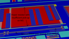
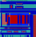
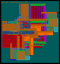
Here are all the images I sent them with instructions on what needs changing...
I think I'm done now, and Treehouse will be done making these edits tomorrow. Then, I'll get a new .gds file to review.
Here are all the images I sent them with instructions on what needs changing...


Comments
The guy that did this work is about 25 years old and he lives near Mexico City. The layout tools tell him when he's made a design-rule violation or didn't match my schematic. He relies on those tools to do his job, of course. The crazy thing is that he doesn't know electronics! He doesn't really need to, although that knowledge would have saved the need to make so many edits, in this case. Had I thought to put explicit wire-width instructions into my schematic for him, he would have followed them. I just assumed that if he saw a wide, multi-gate, min-length transistor, he would know to increase the metal connection widths, but that wasn't the case.
In the end, he did a pretty good job and there were just a handful of things that needed revisiting. I've spent days tracing out high-current signal and power routes, making sure they are sufficient, or finding ways to make them sufficient. I think we've got them all fixed now and this layout is production-worthy.
EDA tools are leaned on heavily by chip designers, these days, to let them know if they have done things right. If the tool tells them they're done, they're done! The tool just checks for design-rule compliance and schematic match, without regard to things like an air compressor being plugged in via two series'd lamp extension cords. This is a funny by-product of skill specialization. It never occurred to me that the person doing our layout work wouldn't know electronics. He did a lot of work pretty quickly, though, and it was generally high-quality. We just had a few things to patch up, in the end.
(and be low-risk....)
No, we've been holding up the shuttle. These are going into the test chip AND the production chip.
One thing about layout, though, is that it's about the only aspect of chip design that can be delegated - except for synthesis and integration, which is another huge task. If I tried to do layout, also, I wouldn't have enough time for everything else that needs to get done.
I would say, "that's crazy!", but I'm seeing similar things in the mechanical realm too. Sharp guys who know CAD, can process rules, geometry, use the tools...
Did a design review on a simple sheet metal enclosure a couple weeks ago. I was kind of stunned to understand the guy laying out all the parts has never made anything at all!
And sheet metal is kind of simple. Even so, there are considerations. Not too many of them, but enough to show the difference between having some understanding and not.
For the cost of this stuff... I am consistently shaking my head in wonder at just how much of the real value has been taken out of things.
When we were building automation and packaging up experience into software, etc... (and that packaging of experience = design rules and other constraints / parameters), the idea was originally to empower people. Free them to do more, better, faster.
I believe in that, and have managed to do it a time or two, and do it exactly that way. Mostly the same people, maybe let a couple at the bottom go, but not this massive reduction we see all the time. Those people free to actually experience the job, learn, improve and take all that software, automation as extensions of themselves.
Instead of doing work cheaply, lean, efficient, no BS style, they could be doing great work, cheaply, lean, no BS style.
Everyone benefits, and it's not such a race to the bottom.
But, what we get is marginal, to "just good enough" work, not always lean, usually efficient, and with more BS these days than is needed.
And the cost reductions are significant. No joke there.
Until... one costs out what missing experience can cost us. And what not passing it along does too. We are gonna have a generation of people who just can't do what we do, know the kinds of things we know.
Not sure how I feel about that. Frankly, I can do most of what I've done in life without a computer. Old school. It's not pretty, but the basics are there. True for a lot of you guys too. I can tell.
Programming aside, that's a computer thing. Except for something Heater will surely tell us.
And as these great tools have come along, my time has been freed to do much better work! Kind of awesome. And I got to train lots of people too. Good, except for I've come to learn most of them boiled it down to the nubs, didn't actually practice the art, skill, physical bits as I did, instead leaning hard on the tools, working for less, slamming out much more, quality just not there, nor is consideration a lot of the time.
Thanks for sharing this stuff Chip! These layouts are amazing! So darn many parts, so small.
Doing this project with all of you has been frustrating, because it's taken a long time. But, it's been very rewarding too! Have learned so darn much.
Double, triple, quadruple check is the norm here? Anyone else, who does know real stuff, able to take a look? Not that anyone doubts you. It's not that.
Just details. So many of them. I know if it were me, no matter what my skill level actually was, I would be sweating this stuff big!
Is this work being done by the hour or project?
Color me not surprised.
My company has also outsourced loads across the world, and while some areas have outstanding technical people (Eastern Europe), others are just warm bodies.
Absolutely kills me that higher up VIP's are willing to shaft me and our customers with sub-standard work/product/processes with what turn out to not be cost saving measures in the least.
Now that you know where they're short-changing you here, aren't you kind of curious if they aren't short-changing you elsewhere?
During that time the boss of the PCB girls proudly showed me a board that had been laid out by computer. You could tell, any diagonal traces had little stair-steps in them! We speculated how soon all those girls would be out of a job and the engineers could layout their own boards in no time.
Of course what happened is that board design moved to a few PCB specialists that know their tools inside out. Or disappeared into synthesizable HDL for FPGA and ASIC etc.
Just checked TH website and found this:
"As time went on, it became clear that to deliver best-in-world value to our customers we would need to look globally to find world-class expertise at globally competitive rates, "
World-class expertise in IC layout, by someone who doesn't know electronics?
Dig into the contract and see what the hourly rate is for this "expert's" work.
EE in Mexico City average is $31K, Graphic Design 14K, so assume that employee is around $7-15/hour cost to TH at most.
Well, I guess I can understand why the MBA's have the ear of so many CEO's now.
Seriously, I was replaced by that? ... I give up. You might be able to get away with automated digital layout without knowing any electronics, but with any analog layout designer worth their weight, you absolutely must have quite a bit of knowledge, theory, and experience to back what you are doing with any degree of confidence.
I do appreciate the complement Chip ... "Beau was a master at tight layout" ... and there is good reason for that based on the knowledge, experience, and specific schooling at National Semiconductor I received. They say teaching a class in a subject is the best way to reinforce your own knowledge, I did that as well with the Georgia Tech students a part of my career at NSC.
I feel that what you are doing is the wrong approach, you are introducing way too much human interaction with the final layout at this stage in the game. The human verification needs to have been done at the very beginning of the process. It's just way too easy to overlook and miss something that could be critical. Power, Ground, and signal structures need to be planned out first before any real routing can take place to overcome any IR drop that can occur over long distances. You can't rely on an automated tool to do this for you, it just doesn't happen in Analog layout design reliably. Doing this NOW can end up being a painful process with many opportunities for human error to work it's way into the design. Essential additions or removals can easily be missed from the design all together with this annotated approach you are playing with.
Seems like two options to me:
- Do the best he can with whatever Treehouse can provide.
- Or, drop Treehouse, forget the custom altogether, and live within the confines of synthesises only.
I do hope they are not charging you for their mistakes!
I would be seriously ****** finding this out at this late stage in the process!
Exactly
We need maybe only 1/4 full-time layout help. Keeping a guy on staff, with tool licenses, is at least a $120k annual commitment. It's impossible for me to keep him busy and he'd languish for lack of meaningful work. People need to be busy to stay engaged. It's our nature.
At this point, after the fixups, I'm very confident that the layout is good. It's not as perfect as I'd like it to be, like Beau would have made, but it's well within the envelope of what is needed.
Treehouse certainly has stateside staff that are expert in layout, and we could have used them from the start, but at a much higher rate.
The Mexico option was about half the cost! And it's turned out fine, after I pointed out what needed fixing, but had I realized the need for detailed instruction in the beginning, the late fixups would have been largely avoided. He did follow my instructions quite perfectly on concentric array layouts, and such, which are critical. I just didn't realize how much detail he'd need on wire widths. But, really, I should not have assumed that anyone would know what I was thinking.
Within Treehouse, they annotate their own schematics with wire width instructions, since they realize it will ensure that the layout designer will give them what they need.
It’s a little late now but since you’re commenting - based on the interesting projects Beau posted here, Beau was a rare layout engineer who could have contributed in many different areas other than layout. New grads in the valley easily make $120k just in salary, so if your burdened cost for him was that low you had a real deal.
That's the most important part to get the silicon moving, right there. Glad you got it figured out! I've officially joined the hoards impatiently waiting the P2 now, I guess.
Well, color me surprised at that billable rate. Was expecting quite a bit higher.
However, as Heater said, I'd be p***** if I had to pay someone that, who had no clue about electronics and upon which my entire project was dependent.
One doesn't have to think very long or hard about all the other jobs you have TH doing for you, and how experienced the people actually doing the work are.
Who quite possible are not the people who show up at face to face meetings....
Hopefully things work out.
This is all your fault. Move to Mexico city and make another offer:)
Rich
Ken Gracey
I don't know if he was told that. But from what I got from his posts a couple years ago, I thought he was pretty angry. He should know that his work was that good and appreciated.
I wanted to post the above comment a couple of weeks ago after Chip's comment. But I desisted because I thought it was a bit too harsh. I still think so, but in light of later comments, I think your opinion of Beau's work is important.
How true that is !
Meanwhile, I rented an ESD zapper gun, since my old one went kaput, and I've been zapping the prior test chip. It has the same ESD circuits as the new one, so it can reveal any ESD weakness in our design. Surprisingly, the chip failed ESD testing miserably! The problem is that the core ground (GND) and I/O ground (GIO), while normally at the same potential, can get a huge differential during a zap.
The core ground and I/O grounds are not shorted together on the die, but are both bonded down to the exposed pad, which becomes BOTH grounds. This was done to keep core ground currents, which are quite high on the die and cause ~25mV differences on what should be the same "ground", isolated from the I/O grounds which may be doing ADC and DAC operations that would be really compromised by ground noise. Anyway, during an ESD zap, those core and I/O grounds could be 50V apart for a few nanoseconds. This was causing my level shifters to blow out, as delicate NMOS gates were exposed to this havoc.
In order to fix this, I need to add a resistor and a small ESD clamp on each of the cross-domain connections where the NMOS transistors are being driven.
I had plenty of ESD protection where I thought it was needed, but totally missed the other vulnerabilities. Today I'm working on the schematic for the PAD ring elements to fix all this.
That sounds like it will slow signals down ? (and may not give best protection)
Can you not add some 'fat' back to back diodes (one may be there already) between the two grounds ?
In normal operation, they are mV separate, but in ESD event, the diodes ensure the GNDs cannot wander too far apart ?