Boost your Propeller's memory 256x, from 32kB->8MB
in Propeller 1
I use the Propeller to build scientific instruments; see here for details – www.instruments4chem.com
For most of my projects, 32kB of HUB RAM has been perfectly adequate, but there are times when more memory would certainly be useful. I’ve had previous experience using HyperRAM in several XMOS-based projects. HyperRAM is low cost/MB and interfacing to it requires a minimal pin count.
Over on the P2 forum I’ve recently posted some code for a P2 FPGA emulation interfaced to an 8MB ISSI HyperRAM chip. That project provided an opportunity for me to learn how to use some of the great new features on the P2 (streamer and smart pins).
In the absence of a real P2 in silicon, however, the P1 remains my go to workhorse and I’ve leveraged the knowledge gained from previous experiences to now make available a P1 HyperRAM solution.
Here’s a summary of the hardware/software details :
HyperRAM PCB footprint is just 6mm x 8mm in a 24 pin FBGA package
Apart from that, just a couple of decoupling caps are needed
Code is written in SPIN, launching 3 COG’s running PASM to manage the HyperRAM interface
14 pins are dedicated to this interface, leaving 14 free for user applications
Data transfer rate between HUB RAM and HyperRAM is ~1.6 MBytes/sec
(that figure is based on code – see below - moving 24576 bytes between the two)
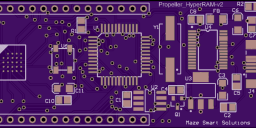
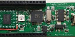
I’ve attached some images to show my setup. My initial prototype can be seen in ProtoHR.jpg. There were a few issues with this PCB that required correcting (hence the bizarre wire link, seemingly connecting Vcc and GND !!) and I’m currently waiting on a new PCB – OSHPark_HR that will address these.
Here, header J5 breaks out 3.3V, GND and Propeller pins P0-P13, and J6 : 3.3V, GND and P14-P27. I’m currently making some shields that plug into these headers but i'll say more about those in a future post.
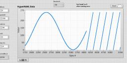
The other two images (LabVIEW_HR and LV_HR_Expanded) show a LabVIEW screen; here my PC is interacting with the Propeller via its on-board FT232RL. Here’s what happens :
On launch, SPIN code first fills a 24576 byte array with 6 different math functions (6 x 4096 bytes).
This array is written in its entirety into HyperRAM as 1536 (Repeats16) x 16 byte buffers, then is read back into HUB RAM, then uploaded to the PC and displayed into the “HyperRAM Data” graph window. BTW I refer to each of these buffers as a “block”.
That whole process then gets repeated 340 times (the Iterations field) – resulting in a total of 8,355,840 bytes being moved back and forth between HUB RAM and HyperRAM. During such a run, the current block field is constantly incrementing by 1536 on each iteration.
Data integrity will be maintained throughout the run only if the data transfers are rock solid. I’ve used the continuous running mode in LabVIEW (its double arrow button mode) to exercise the above sequence over and over (tens of hours) and so far it’s all looking good.
A couple of other things :
The SendC field here is set to 1 the very first time this vi is run – that sets up the two HyperRAM configuration registers CR0 and CR1.
Delay/ms provides a LabVIEW delay between issuing HyperRAM write and read commands - which for 1536 of these 16 byte buffers each take a tad over 15 msec.
I’m currently working on documentation - I'll post my code here in the next couple of days.
Finally, in closing - there’s now a dual die stack 16MB version of HyperRAM (!!) ; I’ll be exploring that when I get my new PCB – but I expect it will be fairly straightforward to get working since it will have exactly the same interface.


Comments
A great match for P1 & P2.
HyperRAM (1,2 or 3) should work very well as a frame buffer, as the refresh time is 64ms MAX, and that's above most frame times.
With a frame-playback inside that time limit, you do not need to have background refresh, and HyperRAM driving is simpler.
This use is not yet proven on P1, but it should work.
Probably better suited to LCD than VGA, but the basic principle is identical, LCD just allows 'fatter' frame flyback times, and so give more write-during-blanking time.
This would be excellent for P1 as well. We may be able to use MOVS to move and mask at the same time. Of course, it masks 9 bits instead of the 8 we want, but if P8 is CS* it's guaranteed to be low during data transfers. P9-P11 don't seem critical.
16 clocks/long to read data
32 clocks/long to write to hub
4 clocks/l to update address
If a transfer is in progress the hub address could be stored in PHSB and incremented by the clock pulses. The instructions would be interleaved in an unrolled loop. Transfer rate neglecting the preamble would be 6.6MB/s.
It would also be exciting to NOT interleave the read and write. Just read the data in as fast as possible and return the HyperBus to idle so another cog can use it. Has the additional benefit of reading as much data as possible in the 4uS interval. 20MB/s to cog ram and 8.8MB/s to hub ram. Overall transfer rate 6.1MB/s, again neglecting preamble. Transfer rate should increase in nearly linear fashion by adding cogs, approaching 20MB/s.
The next step is to support more than one frame, and with a 64ms Chip refresh time, and 16ms raster time, you can have 4 frames to manage a spread refresh
Others will need to adapt this to suit their own needs - but the code should serve as a useful guide. It hardly needs stating that any parts of the code that directly interact with the HyperRAM chip are very time critical. Seeing SaucySoliton’s previous post (assembling longs, rather than transferring bytes as I'd done, plus a couple of other neat ideas) makes me realize there’s opportunities for significant improvement - so just view this as a first draft...
Currently I'm using my Propeller+HR to develop a LV-based, time-resolved spectroscopy system. It will acquire several thousand scans (each scan is 2048 pixels = 4096 bytes) with each scan captured every 2-3 milliseconds from a linear CCD-based spectrometer into HyperRAM and then upload and display the recorded spectral data as a 3D plot of Intensity vs Wavelength vs Time.
I want to use this to look at time-resolved emission from flames – i.e. an up-market version of the flame tests that some may remember from high school Chemistry days.
OK obviously I'm not understanding something here. If you have a 60 Hz refresh rate, and therefore need to be able to write/retrieve a new frame to/from the buffer every 1/60th second = 16 ms, then aren't you blowing that access rate by 50 ms?
It is so far inside, you could even use up to 4 x 60Hz frames, for distributed refresh, if you wanted to. Something like do one quarter of the not-currently-displayed memory area refresh, in each flyback time.
You still need to allow some time for the user to write to update the frame buffer, so another simple design approach, would be to allocate one frame in 2 for other-refresh, and one in 1 for write time slots.
I was thinking about the latency clocks. Is there any reason the clock needs to be a constant frequency? Reading the datasheet, I don't think there is. In that case, we can boost the clock frequency quickly satisfy the latency clocks. No guarantees how the chips will actually behave. Trace 1 is clock, trace 2 is a data bit.
Escher, do you mean 1 transaction of 16-64 bytes, or the entire 8MB chip? At the current transfer rate it's 5 seconds for the whole chip. Per transaction, I calculated 10uS per 16 bytes from the transfer rate in post 1. There are still a lot of optimizations possible.
Your RIGOL traces (yellow - clk, blue - dat) aren't quite that sequence at this stage but trace 1 does clearly show the higher frequency clock in the latency interval that you are suggesting.
The latency clocks will naturally be faster in any software solution, as they do not need to R/W data bits, and you can reduce the number of latency clocks in a couple of ways.
a) Config the device to the smallest possible latency.
Default is 6, but it can lower via Configuration register to 3 - It is a pity Cypress did not think to allow < 3 here.
tACC also needs to be met, but at 40ns over (min) 3 clocks, that's 75MHz - not an issue for P1, which will be much slower than that.
b) Choose between fixed (simpler but slower) or RWDS poll