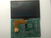
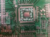
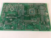
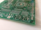
New boards in for my project P1+Max10m25
in Propeller 1
Finally had some time to work on this P1+p1V test board some more. This is a commercial gadget with 7" LCD using the Newhaven display.
P1:
2 HyperRam
2 SPI Ram
1 SPI Flash
1 64k eeprom
1 RTC
1 RS485
Micro SD
P1V Max 10
2 HyperRam
2 SPI Ram
1 SPI Flash
1 64k eeprom
Micro SD
Jtag header
EVE2 LCD Driver
Wifi RNxxx
Xbee Zigbee S2C
Silabs CP2110 with multiplexer switch to select which device to load from the loader app.
If it works, then I can make up the Max10M25 only board later, it would not fit the current panel order.


Comments
Have you been following the work of ersmith ?
http://forums.parallax.com/discussion/164187/fastspin-compiler-for-p2/p1
& some comments/examples here
http://forums.parallax.com/discussion/164708/new-release-propelleride-propbasic-fun-times#latest
That should allow you to code in Spin, then generate either P1 or P2 ASM for quick tests on both cores ?
Addit : And not just in Spin, looks like you can do test code in any mix of Spin and ASM for P1/P2
This from the other thread :
Bumping for progress reports, esp on HyperRAM ?
I did notice latest data says this, which is good news as it suggests > 1024 bytes(1 Row) can stream gap-less.
" When configured in linear burst mode, the device will automatically fetch the next sequential row from the memory array to support a continuous linear burst. Simultaneously accessing the next row in the array while the read or write data transfer is in progress, allows for a linear sequential burst operation that can provide a sustained data rate of 333 MB/s (1 byte (8 bit data bus) * 2 (data clock edges) * 166 MHz = 333 MB/s)."
I've also been thinking about Read/Write in a VGA System, and I see maybe 3 levels of design, where even a P1 could do useful work with HyperRAM.
a) P1 + HyperRAM + CMOS Octal Buffer
Octal buffer gives blanking while write, and more drive, and isolates the pins more.
b) P1 + HyperRAM + QFN32.Logic ie XC2C32 (21io, ~$1.30) OR ICE40LP384-SG32 (21io, ~$1.33)
A little more logic, can allow maybe Sync on Green, to permit smaller VGA connector options, and BG-Colour-force for higher write bandwidths.
Might also fit a faster FG.BG.8pN write state engine. (tho that will be tight in XC2C32)
Probably too small for a CLUT, even in ICE40LP384
c) P1 + HyperRAM + QFN48.Logic ie ICE5LP1K-SG48 (39io, RAM,3x Logic of b) ~$3.28)
The shift from QFN32 to QFN48 bumps the price, but adds significant logic & adds 64kb RAM, which would allow a CLUT, to permit one HyperRAM to map 256:16/18/24b colour for VGA and LCD use.
39io is very close to allowing a Bridge-Design, where 1 RAM is used as CLUT and 1 RAM as Write-buffer, to support write during display & gets close to having the HyperRAM act dual-ported.