

How I use a 40W Laser and a ShopBot to make PCB Prototypes
 JohnR2010
Posts: 431
JohnR2010
Posts: 431
In a Previous post a couple of people expressed interest in how I make PCB prototypes on my 40 Watt Laser. I made a couple of boards this morning and took some pictures so I thought I would share.
Steps I follow
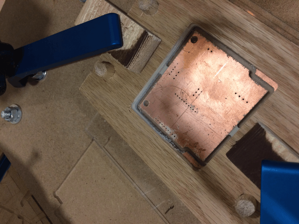
1) Cut and drill boards with my CNC router. (ShopBot CNC)
2) Clean boards and paint with brown primer
3) Let boards dry under heat lamp for 48 Hours
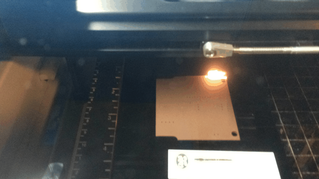
4) Burn away paint with laser to expose copper for etching (Epilog 40 Watt Laser)
5) Etch boards
6) Second Burn with laser to remove paint from pads and clean boards again
7) Tin the pads with liquid tin.
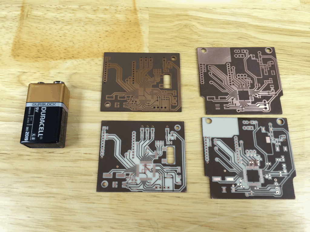
The boards on the top have had the paint burned away and are ready for etching. The boards on the bottom have been etched and had their second burn to expose the solder pads.

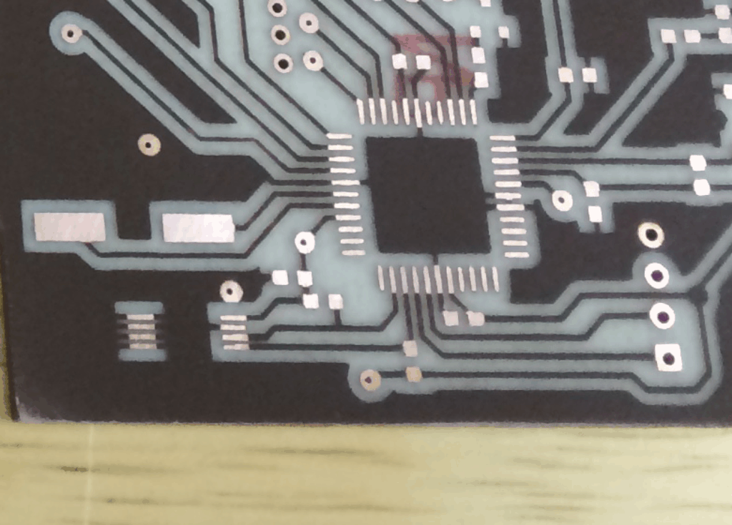
Close up.

Completed circuit of the board on the left of the top photo. This circuit uses an xBee to connect the Propeller to a ZigBee HA network. It uses the Analog cluster to display analog values from sensors. At this point it is waiting to be bound to an analog server.

Cutting and drilling PCB on CNC Router:

Burning Paint away for etching with Laser:

Steps I follow
1) Cut and drill boards with my CNC router. (ShopBot CNC)
2) Clean boards and paint with brown primer
3) Let boards dry under heat lamp for 48 Hours
4) Burn away paint with laser to expose copper for etching (Epilog 40 Watt Laser)
5) Etch boards
6) Second Burn with laser to remove paint from pads and clean boards again
7) Tin the pads with liquid tin.
The boards on the top have had the paint burned away and are ready for etching. The boards on the bottom have been etched and had their second burn to expose the solder pads.
Close up.
Completed circuit of the board on the left of the top photo. This circuit uses an xBee to connect the Propeller to a ZigBee HA network. It uses the Analog cluster to display analog values from sensors. At this point it is waiting to be bound to an analog server.
Cutting and drilling PCB on CNC Router:
Burning Paint away for etching with Laser:
1024 x 735 - 380K
1024 x 768 - 385K

1024 x 768 - 552K
1024 x 576 - 308K
1024 x 768 - 538K

1024 x 1557 - 739K
Comments
Now I need a CNC router and an Epilog laser.
Sandy
If you want to cut resist drying time to minutes instead of days, you might try Cermark LMM-6000 spray. This is a positive process, in that the laser fuses the coating onto the board, and you wash the remainder off with water. After etching, the remaining Cermark can be sanded off. The stuff's pretty expensive, but it does provide a durable coating. You could even make a second application after etching to form a solder mask.
-Phil
Phil, I have done exactly that and it didn't work for me. When I tried, my etchant ate both the CerMark and the copper it was a black soupy mess. I use CerMark all the time on Aluminum to label our products I would love to use it for this.
I wonder what I'm doing wrong?
I just got my bottle of CerMark and yep it is LMM-6000 Metal Marking Material. I use Ferric Chloride to etch is that what you are using??
As for the pad/hole reregistration that took some time. I think the best thing I did to help with the hole alignment was make the jigs that hold the boards on both machines out of the same DWG file. The first time I burn a board I always make two. I have to move the graphics to get the holes to lineup with the pads. I usually burn a hole stop the laser make changes then try again. The first board turns out being a little off but in most cases still usable. The second board will be dead on like your seeing here.
A word of caution about your CO2 laser and copper...
Copper is 100% reflective in the CO2 10.6um frequency, so there is very high energy flashback with a lot of damage potential to your expensive equipment! The optics would be the lowest cost damage, but anything along the beam path is at risk, especially the laser source itself.
In fact, copper is the material of choice for the mirrors used in the Synrad laser tubes within my CO2 equipment. I was told that copper was one of the few "never in the beam path" materials.
Please take this as friendly advice, but from a rock solid source... Synrad is a world leading CO2 laser manufacturer of 30 years.
Tim
Marty
I think the risk of damage is pretty small. Remember that the laser cutter produces a highly convergent beam at the last possible place in the optical path. The beam focuses tightly on the cutting target but just as quickly diverges again. So any reflected energy is unlikely to be concentrated enough to damage anything.
-Phil
I'm with you on the reflectivity of copper. I have etched mirrors, brass, and aluminum for years with my Laser and it works great. The manual gives sample speeds and power settings to do this. In fact it came with sample brass plates and aluminum with instructions on how to etch it.
Not a bad idea on the oven! 2 days is not that bad as I almost always have to order parts and here in Illinois Mouser takes about 3 to 4 days to get it here (if I go the cheapest route on delivery). Digi Key is a little quicker.
Thinking about it is this the right forum, PCBs can be used for other chips (or is that
heresy!!)
I use Rustoleum Flat Brown the product number is 239112. I have tried several other colors and this one gives me the best result. Other colors have not been as easy to clean off the board after the burn process.
I wasn't sure what forum to put it on but since the PCBs I made are for two Propeller projects this forum has been helping me with I thought it would be okay.
Well it just might work. If you find something your happy with please share. I'm not big on this brown color. I have tried blue, white, and red all from the same family of paint nothing works as good as the brown.
Board File Creation
1. Export from PCB Layout. Create circuit as normal and in PCB layout try to use as many copper pours as possible to minimize etching area required.
2. Export into Corel Draw (for laser etching the paint). Export 5 files one for top layer, top Solder mask, bottom layer, bottom solder mask, and silk screen. Prepare a layer for export by deselecting all objects except Pads, Vias, Traces, Copper Pours, and Board.
a. Under File Preview check Negative then hit save, Saves As Bitmap, Resolution 1000dpi
b. Do the same thing with the bottom layer but also mirror the image.
c. Create the Solder masks by unselecting Negative and only having the Pads, Vias, and Board outline checked. Do this for top and bottom mask
d. Create a Top Silk to make a label to be placed on the board by selecting top Silk and repeating above process
3. Export to PartWorks (for cutting and drilling of board). Export 1 file containing board outline and drill holes.
a. Under File Export DXF select: Drill_Top and Board Outline on left side of window.
b. On Right side you can take the defaults. Hit export to create dxf file.
4. Import into PartWorks
a. Open the xbProp-4x4-pcb template and import the file created above with file import vectors.
5. Import into CorelDraw
a. Open the xb_Prop_PCB_4x4.cdr template
b. File, Import each BMP to the correct tab and resize to 3.6" for both horizontal and vertical dimensions
Here are the settings for the paint burn on my 40 watt laser:
These kinds of posts make me wish I still had all my PCB making materials at home. I loved etching my own ever since I learned back in 9th grade Electronics class (1987)
I did not use CorelDraw, but rather printed my gerber directly from GCPrevue to the laser. Been meaning on making an instructable for that for 2 years now and still haven't. I have a colleague that has been experimenting with some options in Altium to make gerber layers cleaner for laser needs, but we have been focused on building our Shapeoko CNC, so haven't done more with the laser pcb concepts.
I also make "fake PCBs" for test fits for enclosures, test fixtures, and connectors like this: