Towards a P1V Smorgasboard
 Tubular
Posts: 4,774
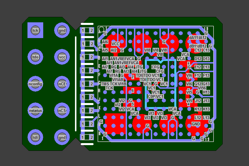
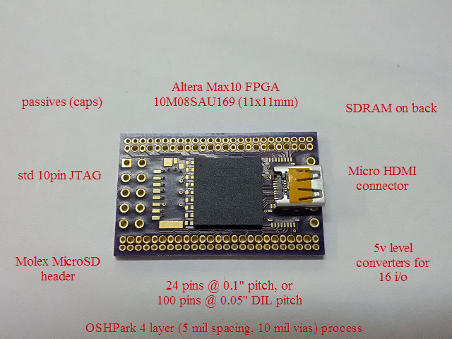
OzPropDev has been doing a great job reducing barriers to adoption on the verilog aspects of P1V. Here are a few designs in progress that might help on the hardware side. They're based on the Altera Max10 10M08SAU169 which only needs a single 3v3 supply rail and is 11x11mm, and reasonable priced in qty 25 at digikey.
I'm using the OSHpark 4 layer (5 mil track/space, 10 mil via) process
These are the designs so far
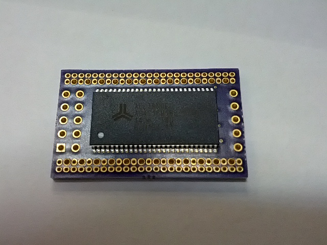
1) A 24 or 100pin, p1v with sdram underneath, microsd header, 5v level conversion or hdmi connector. Not sure whether hdmi video out will actually be possible yet.
2) An 'eeprom' format p1v in DIP8, has an optional Soic-8 eeprom underneath, for easy retrofit to p1's that have an eeprom socket. The p1v sits on the i2c bus
3) A 'qfp' format p1v in 44 pin QFP
there are two other modules I'd like to get to
4) A 40 pin DIP which would be like the 24 pin DIP but perhaps add usb
5) A MCP3208 ADC, DIP-16 format module for picking up 8 analog inputs
The jtag headers will snap off after firmware (altera) programming
I'm looking at using screaming circuits to assemble these in the USA, which also allows other smaller bga components. For small runs (3 oshpark boards) they're not much more than a locally made stainless stencil costs here
If anyone else has a design they'd like to include, let me know.


Comments
I like the idea of the snap-off JTAG header too.
Being a "Patron of the Smarts" and buying at least one of most of the things you "smart guys" make, you can probably count me in for a couple. It looks like a fun way to play with custom P1Vs and maybe even deploy any interesting designs that come about.
Does the "snap off" "snap on" in any form in case you need to refresh the FPGA image?
Keep us informed!!
I don't think snapping jtag back on will be easy, but could at least provide some pads on 25 or 50 mil pitch so it can be lined up and soldered again. That might work.
Looks cool. I see a 10M16 comes also in the 169 pin package. (when released)
I'd suggest adding 25p BGA ( 1 ? 2 ? ) footprints under the SDRAM for the Spansion Hyperbus parts.
They claimed Hyperflash would sample in 2014, and the more interesting 64Mb HyperRAM in Q215
Their DOCs claim a industry std footprint, based on a Dual-QuadSPI .
It doesn't need to literally snap back on.
Nuvoton had the best Idea I've seen in this area.
They have multiple slots in the break off area, and per slot 2 trace pass (1 top & 1 bottom ) thus 5 such narrow channels exist, but those traces can be as wide as the snip part of the web, and can be re-joined with a little care.
Easy to add some structural-only joints ?
I think I understand what you're saying about the bridged tracks, jmg. Need to find the diameter of the oshpark internal routing bit to see whether that'll work with oshpark, or it will end up being quite wide (relative to just tracks).
Hmm. the SPI parts say this "B = 24-ball BGA 6 x 8 mm package, 1.00 mm pitch"
Here is a photo of the Nuvoton Approach to 10 pin PGM/breakoff
http://media.digikey.com/photos/Nuvoton%20Technology/NUTINY-SDK-NUC123.jpg
+ + + 28nm, small size (10x10mm), enough gates for a full P1 (16,640 cells), plenty of RAM 900Kb (@315-500 MHz)
- - - High quiescent current, high price
The Altera parts don't have enough RAM. Max 10M16 doesn't have enough block RAM to fit a full 8-cog P1v. And Max 10M25 doesn't have a 11x11mm package.
(PS: Take a look too to Lattice XP2-5 and XP2-8 in CsBGA-132).
I am going to have to look into Screaming Circuits and Oshpark. Have been limiting myself to the lesser EQFP144 Max 10 Chip package as I figured I had no way to solder a BGA package.
With only a 4 layer board you must be doing some interesting tricks to get access to all of the balls, that is tight spacing to get traces routed around. Or does Oshpark offer blind vias for internal routing? I have been using 4PCB to make my boards and in their 4 layer affordable offering they don't offer blind vias.
How hard would it be to do a version with the F256 17mm 1.0mm pitch BGA package? That one is pin compatible with every Max 10 variant except the smallest 10M02. Unfortunately it is a dual voltage version, but being able to mount 10M04 to 10M50 devices on the same board might be worth it.
If only Altera offered the single supply 10M50 in the U169 package...
Yes, sad they didn't asked anyone on this forum first before their release. Max 10 packaging is not P1v friendly and Cyclone V are expensive.
Another one ... best Altera non-BGA part easy for QFP package:
EP4CGX15BN11C8N $23.96
11x11mm 148-QFN (Exposed pad)
14,400 Cells / 552,960 Kb (not full P1v, but near)
72 I/O (gigabit transceiver !)
Kerry, no blind or buried vias but just 18 mil OD, 10 mil hole vias, which is the minimum oshpark offer. I think its good enough for 0.8mm pitch bgas but wouldn't be fine enough for 0.5mm bga packages. Thats a shame because the level converters are available in compact 0.5mm bga packages that would fit nicely.
and how are you going to control the SDRAM (Quartus doesn't have the IP by default)?
Great info, thanks!
Well I guess I will try my hand at doing a test fit for the F256BGA package. If I could get that on my board it opens up a LOT more potential as then I have the I/O (176) for 96 Prop I/O + a Ram controller... fun stuff.
Goal would be a small board with 4 - 2x20 headers with a Prop I/O bank on 3 and the 4th for optional hard process I/O using any left over pins. There are dev boards out there, but they have junk on them I don't need/want and don't give access to all of the available I/O (how crazy is that?).
With the EQFP limited to 101 I/O I don't have the extra I/O for external ram which would be nice.
If doing a SMD module, dual supply is less of a brickwall, and it can spread the thermal load.
You can say that again... goes from $27.00 each for a 10M08 up to minimum 5 10M50 at $138.00 each ! ! ! Ouch. Really just need a 10M25 but those are so far off it will be next year or later before they are available.
Nice thing with the BGA is I can start with a cheap 10M08 on the board to test out my custom core/mem setup and once I am happy replace it with a 10M50 and its Turbo Time! The EQFP does not share the same pinouts so I would have to make two boards to do that with it
Wish someone would make a GENERIC breakout board for these, just FPGA, Power, RAM and I/O Headers and nothing else (well maybe a USB/JTAG connection for easy programming). Altera has a 10M50 board coming out for only $199.00 BUT it has almost no user I/O on it as it is taken up by demonstration features that I don't want or need.
The level converters - TXB0108 (or TXS0108)
Regarding the SDRAM, still working that out. It seems Alera's premier IP block is for DDR2/3. Not sure whether that means there is a different IP block that just does SDRAM, or what. My main concern at this stage is to use the right pin connections.
Agreed, this is really what's needed to embed into products. Its also what Parallax used to sell some time ago.
http://www.orientalcommodities.co.uk/P/BR838002Big.jpg
Another approach to this, is to have 'SMD connector' like pads on the PCB end, that edge-solder a std 10W Box header. This has tolerable PCB real estate impact, as the 2 x 5 pins fit inside a 0.6" DIP edge, and a not-fitted PCB is very compact.
It could even have a row of holes at the back on 0.05" as the vias & direct ribbon solder option.
The vertical IDC headers are cheapest, and one could even use unshrouded . (with keying pin?)
If the PCB has the connector un-mounted, users have a choice of how tehy manage JTAG connect.
Thanks. I like the specs (can do 100 MHz), and they have a lot of package options. But I have read several comments saying that they easily oscillate (due to their bi-directional autosensing) and some people recommend other translators that have pin for direction. Now there are so many translators that is difficult to choose one.
There was a problem a few years back on the Propeller Servo Controller Board
https://www.parallax.com/search?search_api_views_fulltext=28830
which used the same translator chips:
http://forums.parallax.com/showthread.php/118121-Digital-servo-s-on-USB-servocontroller/page2?highlight=PSCU+translator
EDIT: added schematic
We'll have a full-automatic Pick&Place soon here!
Maybe there are some that autosense, but spec << 100MHz to make them less oscillation prone.
I guess there is always a mix of i2c Buffers, AutoSense, and Direction Pin parts - if you have room ?
Since its an FPGA with plenty of pins, it would be possible to bring out the individual DIR signals, on the pins in between the physical 0.1" pitch pins. That might make for a compact buffer arrangement just off the main core board, and can be experimented with later.
@6581, will keep you informed!
So the same footprint could also accept 2 x panasonic EXB18V resistor networks, which also have a 0.4mm pitch, and are available down to 0 ohms.
There are also DIP8 pads underneath for a kind of compact 8 pin micro.
The pricing on the Max10 FPGAs has come down in this 11x11mm package
Lattice also have a new MachXO3L-9400, in 9x9 package, and a LFE5U-12 in 10x10, but no prices/stock showing on either yet.
I'm trying to use the OSHpark 4 layer service. Its a bit of a balancing act to get the right combo - really need 0.8mm (or preferably greater) pitch, but still keep within that 11x11mm area, which rules out a lot. Those lattice parts have just a few too many pins in their 0.8mm pitch
I have a reflow oven if you want to give it a try. I haven't tried BGA yet -not willing to risk it on expensive chips
I have been thinking for a long time of making a simple FPGA board using an EP4CExxE22C8N (TQFP144 @0.5mm). The 06/10/15/22 versions are not totally pin compatible as higher density parts swap I/Os for additional PWR/GND pins. Forget the 10 version as the 15 is almost the same price.
I just looked at the Max10 series 10MxxSxE144C8G (TQFP144 0.5mm) again. The 08/16/25 series are pin compatible and the 40/50 series are pin compatible. Haven't checked the differences between the two series.
The Max10 have quite a bit less ram than the Cyclone IV for the same LEs.