

Minimal SRAM Driver...?
 rjo__
Posts: 2,114
rjo__
Posts: 2,114
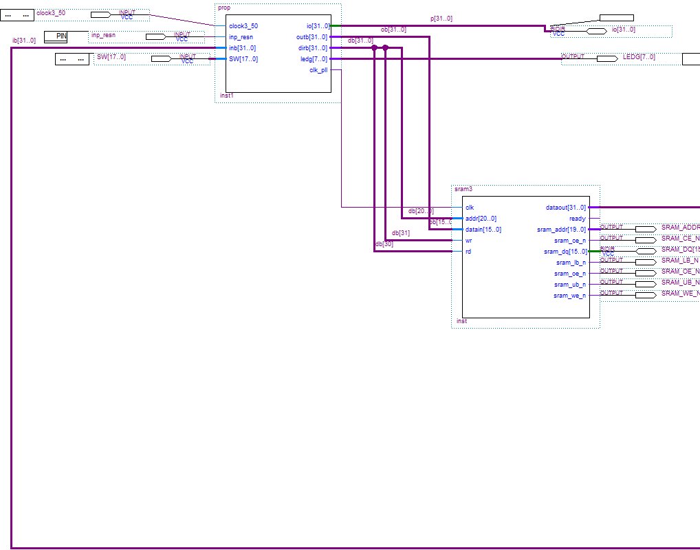
I started with Pik33's instructions for making a block diagram http://forums.parallax.com/showthread.php/156849-Triassic-Prop-(Terasic-DE2-115-Adapter-)?p=1284940#post1284940
then began hacking away at Pik33's VGA9.v until I got down to this:
which can be interfaced in Spin to create a minimal SRAM controller... using almost the same logic as Pik33 does in his implementations.
And it actually works... no problem. BUT there is something that is kind of odd... I have to toggle DIRB[31] ... on and off... and on again... to write. doesn't make sense to me.
any ideas?
Thanks
Rich
then began hacking away at Pik33's VGA9.v until I got down to this:
module sram3 (clk,addr,datain,dataout,wr,rd,ready,      // P1V interface
             sram_addr,sram_ce_n,sram_dq,sram_lb_n,sram_oe_n,sram_ub_n,sram_we_n);// sram interface);
input wire clk,wr,rd;
output wire ready;
input wire [20:0] addr;
input wire [15:0] datain;
output reg [31:0] dataout;
output reg [19:0] sram_addr;
inout wire [15:0] sram_dq;
output wire sram_ce_n,sram_oe_n;
output reg sram_lb_n,sram_ub_n,sram_we_n;
reg [15:0] sramdqout;
reg oldwr,wr2;

assign sram_ce_n=0;
assign sram_oe_n=0;
assign sram_lb_n=0;
assign sram_ub_n=0;
assign sram_dq = (sram_we_n==0) ? sramdqout : 16'bz;
always@(posedge clk)
  begin
  oldwr<=wr;
  if ((oldwr==0) && (wr==1)) wr2<=1; else wr2<=0;
  sram_addr<=addr[19:0];
  sram_we_n<=!wr2;
  if (sram_we_n==0)sramdqout<=datain; else dataout<=sram_dq;
  end
endmodule
// This is free software, license: LGPL v.2.0 or newer
which can be interfaced in Spin to create a minimal SRAM controller... using almost the same logic as Pik33 does in his implementations.
CON
  _clkmode = xtal1+pll16x
  _clkfreq = 100_000_000
  writesram = 1
  readsram =2


OBJ ser : "FullDuplexSerial"
VAR
   long command,address,value,readval
   long startadd
Pub testsram
   ser.start(31,30,0,115200)
   startadd:=100000
   address:=startadd
   readval:=1111
   value:=0
   ser.str(string("hello",13))
   coginit(3,@entry,@command)
   waitcnt(clkfreq/3 + cnt)
   repeat 20
     command:=writesram
     repeat until command==$FFFFFFFF
     address++
     value++
   address :=startadd
   repeat 20
     command:=readsram
     repeat until command==$FFFFFFFF
     ser.str(string("address="))
     ser.dec(address)
     ser.str(string("      returned value="))
     ser.dec(readval)
     ser.tx(13)
     address++

  ser.str(string("Done"))
  repeat

Dat
                      org 0
entry
                             mov paradd,par
                             rdlong a1,paradd
                             cmp a1,#1 wc,wz
                             add paradd,#4
                        if_c jmp #entry
                        if_z jmp #wrsram
                             cmp a1,#2 wz
                        if_z jmp  #rdsram
                             jmp #entry
wrsram
              rdlong    addr,paradd
              add       paradd,#4
              rdlong    data,paradd
              mov       outb,data
              mov       dirb,addr
              or        dirb,a8000   ' a8000=$8000_0000 - write strobe bit #31
              andn      dirb,a8000   'clear bit 31
              or        dirb,a8000    'strobe bit 31
              mov       paradd,par
              wrlong    offff,paradd
              jmp       #entry
rdsram
             rdlong    dirb,paradd
             nop
             mov       data1,inb
             add       paradd,#8
             wrlong    data1,paradd
             mov       paradd,par
             wrlong    offff,paradd
             jmp       #entry

a8000 long $8000_0000
a4000 long $4000_0000
offff  long $ffffffff
data    res  1
addr    res  1
data1   res  1
a1      res  1
paradd res 1
And it actually works... no problem. BUT there is something that is kind of odd... I have to toggle DIRB[31] ... on and off... and on again... to write. doesn't make sense to me.
any ideas?
Thanks
Rich
1018 x 800 - 80K
Comments
In the verilog code... we have sequential logic... a three clock sequence, which is triggered by each transition of wr from low to high. wr is connected to dirb[31].
The Pasm code that creates the trigger for this sequence is:
             mov       outb,data
              mov       dirb,addr
              or        dirb,a8000   ' a8000=$8000_0000 - write strobe bit #31
              andn      dirb,a8000   'clear bit 31
              or        dirb,a8000    'strobe bit 31
If I simply set and clear dirb bit #31, the address of the sram is set incorrectly. Only if I (1)set, (2)clear and then (3)set again bit 31, does the code work correctly.
I have tried reversing the verilog transition to be from high to low...this has no effect... the same Pasm code that works, still works and I still have to reset 31 to get the proper address.
and I have tried inserting nop instructions to see if it was simply a timing issue... with no effect.
I need to understand this, because it will be the basis of an image buffer, whiere wr will be triggered by a pixel clock and I need to get to a minimal sequence before I go there.
Thanks,
Rich
On the other hand... I'm still having trouble with stupid pins... as in the above example:)
Get a vga11.v and vnfg098.spin from 0.98b retromachine; there is source f it in its topic; they are newer and some bugs are fixed
I've also seen cases where High Speed Programmable Logic devices, really do not like slow edges - my guess was the edge oscillations and common mode inductance combined to travel further than expected.
You also should not need 3 writes to a strobe pin, just a clear/set should be ok, as it arrives set with each call.
A RAM WRN pin, should reset inactive.
I'll take a look.
jmg,
The input is wr, which is inverted from the actual output(sram_we_n). So, a single write seems to take -_-_ on the sram_we_n... ,when it should only take -_
Everything else is held low. According to the data sheet...that's all that it should take.
If I do it with a single toggle... somehow the last written value shows up in the first written address....
Problem solved.
always@(posedge clk)
  begin
  oldwr<=wr;
  if ((oldwr==0) &&(wr==1)) wr2<=1; else wr2<=0;
  wr3<=wr2;
  sram_addr<=addr[19:0];
  if ((wr2==1) || (wr3==1))
      sram_we_n<=0;
     else
	   sram_we_n<=1;
  if (sram_we_n==0)sramdqout<=datain; else dataout<=sram_dq;
  end
endmodule
needed to hold sram_we_n low for an extra clock:)
mov outb,data mov dirb,addr ' a31 to zero or dirb,a8000 ' Rising edge on a31 -> Verilog to trigger 2 clk wide WRN on RAMYou are absolutely correct! ... and NOW we have a minimal SRAM driver:)
Thanks
Rich