Shop OBEX P1 Docs P2 Docs Learn Events
Bypass capacitors for the P8X32A-Q44 — Parallax Forums

Bypass capacitors for the P8X32A-Q44

Sir GawainSir Gawain Posts: 32
edited 2014-07-16 06:59 in Propeller 1
Hi everyone,
I am porting a multi-prop project to a board using the 44 pin P8X32A-Q44.
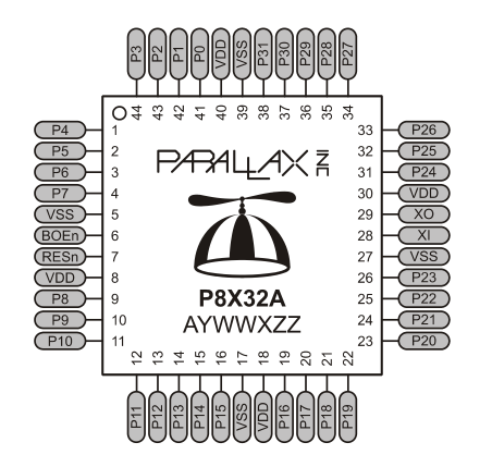
It has a VDD and a VSS on each of the four sides.
This seems to be an opportunity to maximize bypass capacitors.
The thought of putting four equal ones on each side seems appealing, but they might be "in parallel," and in addition to this the Propeller Demo Board and other boards only use one bypass capacitor.

My question is whether it would be advantageous to add a second (or third or fourth) bypass capacitor of a different value?
For example, pins 8 and 5 (of the 44) could have a 1uF and pins 40 and 39 could have a 0.1uF...or any combination on the four sides.
What is the very best that can be done?

I appreciate the input !! :)
P8X32A-Q44.png
452 x 429 - 71K

Comments

  • Phil Pilgrim (PhiPi)Phil Pilgrim (PhiPi) Posts: 23,514
    edited 2014-07-13 11:19
    Add as many bypass caps as you have room for. Four, between 0.1uF and 1uF are optimal. Also, make sure that each Vdd and Vss pin gets its own connection to Vdd or Vss.

    -Phil
  • PublisonPublison Posts: 12,366
    edited 2014-07-13 11:21
    Sir Gawain wrote: »
    Hi everyone,
    I am porting a multi-prop project to a board using the 44 pin P8X32A-Q44.
    It has a VDD and a VSS on each of the four sides.
    This seems to be an opportunity to maximize bypass capacitors.
    The thought of putting four equal ones on each side seems appealing, but they might be "in parallel," and in addition to this the Propeller Demo Board and other boards only use one bypass capacitor.

    My question is whether it would be advantageous to add a second (or third or fourth) bypass capacitor of a different value?
    For example, pins 8 and 5 (of the 44) could have a 1uF and pins 40 and 39 could have a 0.1uF...or any combination on the four sides.
    What is the very best that can be done?

    I appreciate the input !! :)

    P8X32A-Q44.png

    Yes, it is always best to add decoupling capacitors to EVERY VSS, VDD connection on the Prop.

    It does away with PLL failures.

    EDIT: Again Phil types faster than I do.
  • Sir GawainSir Gawain Posts: 32
    edited 2014-07-13 12:39
    Thanks for the quick reply guys.
    I'm using Diptrace and manually placing the bypass capacitors as close to the pins as possible.
    Using the "auto placement" does not always do this little perfection.
    I imagine that one should favour a close + positive over a close - negative...

    At other times, when capacitors are filtering noise, it is beneficial to have a sweep of values.
    Do you think this is worth the effort? Just use bigger values exclusively?
    I am trying to create a pretty nastily little multi-prop...
  • JonnyMacJonnyMac Posts: 9,105
    edited 2014-07-13 13:22
    I always manually place everything, too -- for aesthetics and control. All my bypass caps are 0.1.

    Here's a board I'm working on for a friend. the caps and resistors are 0805s to facilitate building by hand.
    1024 x 576 - 106K
  • Sir GawainSir Gawain Posts: 32
    edited 2014-07-13 13:23
    JonnyMac wrote: »
    I always manually place everything, too -- for aesthetics and control. All my bypass caps are 0.1.

    Here's a board I'm working on for a friend. the caps and resistors are 0805s to facilitate building by hand.

    Very nice !! One could say even inspiring!
    The philosophers ascribe beauty to proportion... :)
  • Cluso99Cluso99 Posts: 18,069
    edited 2014-07-13 14:37
    I put a ground plane under the prop on the top side and a 3v3 plane on the underside. Then on the 3v3 and ground feed in i place a 10uF X7R. From the planes to each of the 3v3/gnd sets on the prop i place a (4x) 0.1uF X7R. All caps are on the underside. Dont forget to place an isolated gnd plane under the xtal going to the gnd pin beside the xtal pins. This makes for an extremely reliable circuit to overclock to 104MHz. While I can achieve 108MHz and higher, I dont in practice use it.

    BTW I am now using 0603 0.1uF caps and i find they are easy to hand solder - just make the pads extend out a bit further and a little wider. I put them on my extended 0805 pads but they are a bit too big and not quite close enough between the centers.

    I use a 4x10K resistor pack for SDL, SCK, RESET and WP pullups.

    I yu use the ssop fine pitch eeprom, make sure you extend the pads out for hand soldering.
  • Phil Pilgrim (PhiPi)Phil Pilgrim (PhiPi) Posts: 23,514
    edited 2014-07-13 17:43
    Cluso makes some good points. I put the Vss plane on the bottom of the board, and it covers the whole board. Any traces on the bottom are kept short and to a minimum, so as not to break up the ground plane. I also add a small power plane on the top side under the Prop chip. In addition to the bypass caps, any bulk capacitance on Vdd should be placed as close to the 3V3 regulator as possible, in accordcance with the regulator datasheet. If 3V3 is coming from another board, a 10uF or more tantalum or ceramic cap should be placed near where the power enters the board.

    -Phil
  • Cluso99Cluso99 Posts: 18,069
    edited 2014-07-13 20:05
    Just to confirm or add to Phil's comments...

    If my regulator only supplies the prop then my regulator is next to the prop and the 10uF can be shared for the regulator and prop.
    If the regulator supplies more than the prop, then the regulator will have its own 10uF, the prop will have its own 10uF, and if you use an SD/microSD it also requires its own 10uF plus 0.1uF.

    My ground plane on the top under the prop extends at the 4 corners to meet the underneath ground plane outside the prop using 4 vias. The power plane under the prop feeds each of the 4 0.1uF caps and then feeds vias which go to the prop solder pads. This makes each 0.1uF cap actually as close to each power and ground pad as possible, and each 0.1uF is really providing that power/ground pin set.

    Note the use of X7R capacitors. Z5U are much lower spec, yet there is almost no difference in price. For 10uF use tantalum or you can use 10uF X7R but not Z5U.
  • Tracy AllenTracy Allen Posts: 6,664
    edited 2014-07-13 20:10
    I agree about the full Vss plane on the bottom, and the mini Vdd plane connecting the 4 Vdd points right under the Prop. The bypass capacitors connect those two planes, very low inductance overeall. I have the capacitors on the top of the board. I'm using 0603 0.1 µF in 3 of the positions, but have taken to a 1206 4.7µF tantalum bypass capacitor on the one side next to the crystal and run the crystal leads in between the 1206 pads. My intuition is that the different bypass will cover a different part of the noise spectrum. Haven't taken the time to 'scope it out for evidence tho.
  • Sir GawainSir Gawain Posts: 32
    edited 2014-07-13 22:09
    Wow that is some great input everybody - the "heavy hitters" !!

    Just want to say: this is my first post and look at the fantastic and helpful discussion.

    Love it. Thanks. :smile:
  • max72max72 Posts: 1,155
    edited 2014-07-14 00:23
    I have a similar approach.
    Massimo
    1024 x 606 - 123K
    1024 x 549 - 58K
  • Mark_TMark_T Posts: 1,981
    edited 2014-07-14 06:07
    max72 wrote: »
    I have a similar approach.
    Massimo

    But you've neglected to use wide traces to the decoupling capacitors :) - low inductance traces are as important
    as having the caps close to the chip. That basically means wide traces, 32mil or more ideally.

    BTW the reason for wide traces in supply and ground wire is usually for low inductance, not because of the
    higher current, since most chips take a few tens of mA and the resistance of a 10 mil trace wouldn't be an
    issue, but the doubling of the inductance that represents compared to a 32 mil trace is important for decoupling.

    I find its usually rather cramped fitting the caps in, and a few signals have to cross under the chip just to
    complicate the ground and/or vcc planes:
    prop-caps.png

    As you see I often put vias on the chip pads to save space, and often these are the only
    components on the underside so can be hand soldered (tombstoning not an issue!). This
    is my best example, often I rely on the planes to distribute the decoupling and only have 3 caps.

    [Oh, and I often use three 0.1uF and one 1uF or similar combination]
    582 x 560 - 41K
  • max72max72 Posts: 1,155
    edited 2014-07-14 06:22
    Mark_T wrote: »
    But you've neglected to use wide traces to the decoupling capacitors :) - low inductance traces are as important
    as having the caps close to the chip. That basically means wide traces, 32mil or more ideally.

    Thanks for the feedback.

    Massimo
  • abecedarianabecedarian Posts: 312
    edited 2014-07-14 08:51
    I was going to ask about placing the caps under the Prop but you answered this before I had the chance.
    Mark_T wrote: »
    But you've neglected to use wide traces to the decoupling capacitors :) - low inductance traces are as important
    as having the caps close to the chip. That basically means wide traces, 32mil or more ideally.

    BTW the reason for wide traces in supply and ground wire is usually for low inductance, not because of the
    higher current, since most chips take a few tens of mA and the resistance of a 10 mil trace wouldn't be an
    issue, but the doubling of the inductance that represents compared to a 32 mil trace is important for decoupling.

    I find its usually rather cramped fitting the caps in, and a few signals have to cross under the chip just to
    complicate the ground and/or vcc planes:
    prop-caps.png

    As you see I often put vias on the chip pads to save space, and often these are the only
    components on the underside so can be hand soldered (tombstoning not an issue!). This
    is my best example, often I rely on the planes to distribute the decoupling and only have 3 caps.

    [Oh, and I often use three 0.1uF and one 1uF or similar combination]
  • Heater.Heater. Posts: 21,230
    edited 2014-07-14 09:06
    I always though decoupling capacitors were like salt on your dinner. Just add to taste. At least that's how I have seen a few "professional" designers handling them:)
  • Mark_TMark_T Posts: 1,981
    edited 2014-07-14 09:54
    Probably out of print, but "Digital Hardware Design", Catt+Walton+Davidson, ISBN 0333259815 is
    the bible I read at an impressionable age. Explains how digital logic really works (each gate switching
    slams a current transient onto the supply rails which causes a voltage due to the impedance of the
    supply wiring. Ultimately too much voltage and your chip glitches. The goal of decoupliing is to
    put a stiff voltage source near to the chip (near means low inductance path), that can absorb the
    current pulse without buckling.
    Pretty much the only property of the capacitor that matters is its series inductance for this reason.
    Well, it has to be stiff enough until the voltage regulator can notice and react to the load-change.
    For CMOS the load doesn't change much in the long term, but if you drive high current stuff like
    LEDs then larger caps are needed as well as the ubiquitous 100nF as the load changes are more than
    short term spikes, and the voltage regulator takes time to adjust measured in microseconds.

    That book is where I first learn of Oliver Heaviside, an unsung hero of electromagnetic theory...
  • Phil Pilgrim (PhiPi)Phil Pilgrim (PhiPi) Posts: 23,514
    edited 2014-07-14 10:10
    Mark_T wrote:
    That book is where I first learn of Oliver Heaviside, an unsung hero of electromagnetic theory...
    ... and the eponym for the Heaviside unit step function:

    325px-Dirac_distribution_CDF.svg.png

    -Phil
  • ctwardellctwardell Posts: 1,716
    edited 2014-07-14 10:37
    Mark_T wrote: »
    Probably out of print, but "Digital Hardware Design", Catt+Walton+Davidson, ISBN 0333259815 is
    the bible I read at an impressionable age. Explains how digital logic really works (each gate switching
    slams a current transient onto the supply rails which causes a voltage due to the impedance of the
    supply wiring. Ultimately too much voltage and your chip glitches. The goal of decoupliing is to
    put a stiff voltage source near to the chip (near means low inductance path), that can absorb the
    current pulse without buckling.
    Pretty much the only property of the capacitor that matters is its series inductance for this reason.
    Well, it has to be stiff enough until the voltage regulator can notice and react to the load-change.
    For CMOS the load doesn't change much in the long term, but if you drive high current stuff like
    LEDs then larger caps are needed as well as the ubiquitous 100nF as the load changes are more than
    short term spikes, and the voltage regulator takes time to adjust measured in microseconds.

    That book is where I first learn of Oliver Heaviside, an unsung hero of electromagnetic theory...

    It is available online, seems to be legitimate site:

    http://www.ivorcatt.org/digital-hardware-design.htm

    C.W.
  • Heater.Heater. Posts: 21,230
    edited 2014-07-14 10:46
    "Legitimate"? That is the famous Ivor Catt we are talking about here.

    Although some of his ideas on EM theory are said to be a bit questionable, if not crackpot, by the academic community.
  • ctwardellctwardell Posts: 1,716
    edited 2014-07-14 10:54
    Heater. wrote: »
    "Legitimate"? That is the famous Ivor Catt we are talking about here.

    Although some of his ideas on EM theory are said to be a bit questionable, if not crackpot, by the academic community.

    Lol, that wasn't a comment on Mr. Catt. I meant that it doesn't look like it's just some schmuck posting someone else's work on the interwebs...

    C.W.
  • Tracy AllenTracy Allen Posts: 6,664
    edited 2014-07-14 11:01
    I've found these articles informative, from UltraCad president Doug Brooks, with references to professional research and standards on the subject...
    http://www.ultracad.com/article_outline.htm
    May be more than you want to know!
  • RaymanRayman Posts: 14,658
    edited 2014-07-14 12:12
    I usually put four 1uF MLCC's, one on each side. But, I doubt it's required. I've seen the dip version work just fine, even put out VGA and NTSC video with just leaded Ta caps, one on each side...
  • RaymanRayman Posts: 14,658
    edited 2014-07-14 12:18
    BTW: In the old days, you'd want to use small capacitor values for bypass caps because they'd have lower inductance.
    But with MLCC, I'm not sure this is true anymore. A 1uF cap is really about the same thing as 10 of 0.1uF caps stacked on top of each other...
    I suppose I could check the rated ESL values, but my hunch is that there is little difference...
  • Mark_TMark_T Posts: 1,981
    edited 2014-07-16 05:03
    Heater. wrote: »
    "Legitimate"? That is the famous Ivor Catt we are talking about here.

    Although some of his ideas on EM theory are said to be a bit questionable, if not crackpot, by the academic community.

    Well this book is just applying Heaviside's telegraph equations to logic signals, and explaining why TTL works
    at all when inadequately decoupled. Its from an era when analog trained engineers were designing digital logic
    boards and getting it wrong (!).
  • Heater.Heater. Posts: 21,230
    edited 2014-07-16 06:35
    Mark_T,

    Its from an era when analog trained engineers were designing digital logic
    boards and getting it wrong (!)
    As opposed to recent times when digital designers were designing analog boards and getting it wrong:)

    When it comes to physical circuits there is no such thing as "digital". The electrons and fields don't know anything about "digital". It has been said that modern fast digital designers are basically working on analog RF circuits.
  • Peter JakackiPeter Jakacki Posts: 10,193
    edited 2014-07-16 06:59
    The main reason for decoupling capacitors on digital circuits is due to the current spikes that occur when switching and with CMOS there is the crossover region where the complementary source and sink pair of every gate etc can be on at the same time, just for the briefest of moments, effectively shorting out the supply rail, plus there is the capacitance of the line and connected gates however small that still needs to be charged/discharged. No matter how good the regulator is it is not able to respond as fast as this (switching logic vs analog regulator = no contest) so fast decoupling capacitors are located very close to the supply and ground pins so as to minimise the inductance which would effectively impede the ability of the capacitor to respond and maintain the supply rail at that instant. If the rail did drop it would affect the switching thresholds as well as lead to possible metastable conditions and delatching of flip-flops/memories, havoc in other words. Switching noise on supply and ground can also find it's way into other parts of the circuit too. It's easier to get a "fast" cap in smaller values which is why you may see 10nF used as well as 100nf plus a 10uf or so (LDO regs are slow).


    I once had a new team of engineers design a new product independently of which they were very proud of as they showed off their wonderful pcb, so full of chips, it must be good, but nary was there a cap in sight. Since they didn't comprehend my head shaking and mutterings I connected the PCB to the scope to show them what the problem was and there was so much noise to be seen, the spikes on the logic rails were measured in volts. See! I said, fully expecting them to go cowering into the corner in shame but to my surprise they still didn't see what the problem was. Ah, ignorance is bliss, but it took them a long long time to sort out all those "software bugs" :)
Sign In or Register to comment.