Analog / Digital Ground Planes 24 bit ADC
Hello folks,
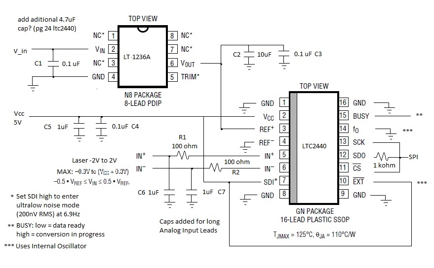
I am once again in need of your expertise and assistance. This is my first attempt at designing a circuit using the LTC2440 high speed 24-bit No Latency Delta Sigma ADC and an accompanying LT1236A 5V precision reference to measure the voltage signal of a high precision laser. For my particular project, 24 bit ADC resolutions is necessary, otherwise I wouldn't bother with all this work.. Layout is very critical for the best noise performance in high precision sigma-delta ADC and the most important aspects I have come to understand is grounding and power supply decoupling (info here on page 6 Layout Section). The power supply decoupling, I believe, I have taken care of via the caps on the REF+, VCC, and AN+/AN-. (If someone could check I would appreciate it). However my main question pertains to grounding. From research (found here on pg 4) I have found that the analog and digital ground planes should not overlap so I will place two copper planes side by side directly underneath my prototyping surfboard.
A quote from pg 4 of the article linked above.
It states that analog and digital grounds should be tied at one common ground point to minimize circulating digital and analog ground currents. Does that mean that these two planes have to be connected? Doesn't that defeat the purpose of separate ground planes?..
Another big question, there are so many grounds in my circuit.. I am having trouble figuring out which ones go to the analog and which ones go to the digital ground planes, especially since I have multiple separate power supplies in the circuit.
V_in into the precision 5V reference is powered via micrcontroller assuming 5V is appropriate V input (not 100% sure from datasheet..)
Vcc (5V) into the 24 bit ADC comes from the microcontroller
Laser Sensor (requires 12-24 VDC) powered via a wall outlet plug
Found a source here on pg 484 saying that when it comes to ground planes, pins in an ADC are a notable exception, in that all ground pins on the IC should connect to the analog ground plane. So does this mean that only the power supply grounds listed above go to the digital ground plane? What if I kept the lase sensors power supply completely separated from the ADC circuit board since it is powered via a wall outlet plug?
Any help would be appreciated.

I am once again in need of your expertise and assistance. This is my first attempt at designing a circuit using the LTC2440 high speed 24-bit No Latency Delta Sigma ADC and an accompanying LT1236A 5V precision reference to measure the voltage signal of a high precision laser. For my particular project, 24 bit ADC resolutions is necessary, otherwise I wouldn't bother with all this work.. Layout is very critical for the best noise performance in high precision sigma-delta ADC and the most important aspects I have come to understand is grounding and power supply decoupling (info here on page 6 Layout Section). The power supply decoupling, I believe, I have taken care of via the caps on the REF+, VCC, and AN+/AN-. (If someone could check I would appreciate it). However my main question pertains to grounding. From research (found here on pg 4) I have found that the analog and digital ground planes should not overlap so I will place two copper planes side by side directly underneath my prototyping surfboard.
A quote from pg 4 of the article linked above.
Analog and digital circuity, including ground and ground planes, should be kept separate when possible. Fast-rising edges create current spikes flowing in the ground plane. These fast current spikes create noise that can corrupt analog performance. Analog and digital grounds (and supplies) should be tied at one common ground point to minimize circulating digital and analog ground currents and noise. pg -4 left side
It states that analog and digital grounds should be tied at one common ground point to minimize circulating digital and analog ground currents. Does that mean that these two planes have to be connected? Doesn't that defeat the purpose of separate ground planes?..
Another big question, there are so many grounds in my circuit.. I am having trouble figuring out which ones go to the analog and which ones go to the digital ground planes, especially since I have multiple separate power supplies in the circuit.
V_in into the precision 5V reference is powered via micrcontroller assuming 5V is appropriate V input (not 100% sure from datasheet..)
Vcc (5V) into the 24 bit ADC comes from the microcontroller
Laser Sensor (requires 12-24 VDC) powered via a wall outlet plug
Found a source here on pg 484 saying that when it comes to ground planes, pins in an ADC are a notable exception, in that all ground pins on the IC should connect to the analog ground plane. So does this mean that only the power supply grounds listed above go to the digital ground plane? What if I kept the lase sensors power supply completely separated from the ADC circuit board since it is powered via a wall outlet plug?
Any help would be appreciated.


Comments
I have no idea about this but one common idea I hear all the time is "follow the current". High current pulses through circuit traces will cause voltage levels to exist where you think "ground" should be.
At high frequencies that means you want very low inductances in those current loops.
Good luck!
Your ADC input filter is odd, I'd just design it as a low-pass RC filter. You will also need to run your 5v reference from more than 5 volts. (5.5v is enough from some modern references, others may need 6-7v) At 1uV voltage levels you also need to watch out for parasitic thermocouples. They can easily generate a few micro-volts of error.
If you want a more stable and precise reference, you can use the LTC6655 in the ceramic package. It's also good to cut slots around the reference to avoid stressing the IC. I've used this reference with a ADS1251 and measured the system noise at less than 2x the datasheet value for the ADS1251 alone.
Marty
You'll need the DC590B (think of it like a prop plug) - another $50 - but can be used with lots of other LT products
Buying the manufacturer's board is an excellent idea. And expecting to build at least 4 layers, and maybe several more to get quiet operation is reasonable. But the process is trial and error.
In general, the Vref needs to be filtered and isolated from the Vdd, likely with a separate ground plane in the Vref region.
24-bit accuracy would be hard to do, but 24-bit resolution is more about dynamic range, so all you have to do is keep
noise down so when you are using the bottom 16 bits it isn't swamped in noise. Here it looks like 24-bit accuracy
is necessary (unlike a lot of audio ADC applications).
All analog ground separate from all digital except for a common point directly under the ADC chip is the usual
strategy. You can join grounds via ferrite beads to reduce RF noise injection. You can join with back-to-back
schottky's so that they float w.r.t each other (within 0.3V bounds). Avoid ground loop by isolated supply to the
board and opto-coupler outputs?
I will take everything said into account and will definitely have a lot more questions about your comments once fine tuning begins. For now, I have assembled my circuit with SMT components (caps/resistors) as close as possible to the ADC chip. I have to say, soldering the 16 pin (.5mm pins spaced) ADC chip was one of the hardest things I have ever done.. even with a microscope I was having a tough time. I also soldered the Precision Reference and positioned it a little above the ADC chip to minimize noise. So for my initial testing, I decided to go with one copper ground plane directly below my circuit (picture of setup attached). Since I did not purchase the demo board (which I also agree is an excellent idea) I will move on with my current setup but will definitely consider purchasing it if I run into any major problems.
So going back to my original circuit design and with regards to this comment:
On page 23 of the LTC2440 manual under the section "Longer Connections to Low Impedance Sources" it states that if longer analog input lead lengths are unavoidable (which they are from my laser), adding an input capacitor close to the ADC input pins will average the charging pulses and prevent reflections or ringing. So I did add 1uF caps on both AN+ and AN- pins.
However in the LTC2440 demo board manual, a 100 ohm resistor is added onto these AN + and - pins in addition to the caps so my final design included both a .1uF cap and 100ohm resistor on each pin.
Obviously there is going to be a voltage drop across this resistor, which is not what I want and which I forgot to take into account, since I want to maximize the voltage range I am measuring.. You mentioned a low-pass RC filter? Would this be better than just the .1uF caps alone on the Analog IN + and - pins? My sensors voltage ranges from -2V to 2V which is within the bounds of -Vin/2 to Vin/2
Thank you
I tested, re-tested, and re-re-tested my original 24 bit ADC handmade SMT prototype board and although it was an EXCELLENT learning experience, I still had trouble getting down to the 200nV noise level specifications stated in the LTC2440 manual. However it is possible to create a handmade board satisfying those specs, as someone demonstrated here, as long as you have excellent soldering skills, a little patience, and an understanding of the fundamentals in high resolution ADC circuit design.
As many of you suggested I went ahead and purchased the DC570A - LTC2440 Demo Board. The satisfaction of seeing stable ADC values at excellent resolution made it worth every single penny! The ADC demo board works great and I am now able to finalize my implementation of this laser sensor in my system.
Once again, thank you for all the help and advice. If you guys have any questions with regards to coding/working with this particular ADC please let me know. Linear Technology has excellent support and sample codes available (written in C for the Arduino) on their site found here.
Thanks again!
Best,
Rob