

PCB layout?
 rjo__
Posts: 2,114
rjo__
Posts: 2,114
This is my first attempt at PCB layout:)
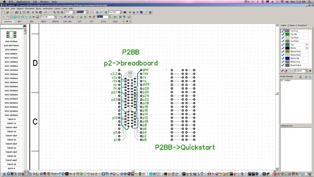
The idea is to design two through hole boards, the first adapts the PCIe4X so that it fits a breadboard. The second board adapts the first so that QuickStart add-on boards can be used with the P2..
I began this before the Expo.
In his Skype call, Chip mentioned that Parallax would offer both of these capabilities... breadboard and 40-pin quickstart pin adapter. So, I think
the only thing I am going to actually have to make is the second little adapter, which can be made by modifying a VeroBoard.

What is wrong with this?
Rich
The idea is to design two through hole boards, the first adapts the PCIe4X so that it fits a breadboard. The second board adapts the first so that QuickStart add-on boards can be used with the P2..
I began this before the Expo.
In his Skype call, Chip mentioned that Parallax would offer both of these capabilities... breadboard and 40-pin quickstart pin adapter. So, I think
the only thing I am going to actually have to make is the second little adapter, which can be made by modifying a VeroBoard.
What is wrong with this?
Rich

1024 x 576 - 97K
Comments
I'd make the power supply wires much thicker where you can (or a copper pour for each half), as the prop 2 could take a fair bit of current.
I haven't checked the pinouts/pin use carefully but it seems about right.
P.S. Why is 'dip' not an acceptable forum file attachment?
Rjo, there is something weird about the pad near the P29 text. It looks different to all the other signal pads.
My idea was to do minimize all the pads that weren't connected (as a later reminder that I didn't have to solder it). I got deflected after changing the first and then forgot all about it until you mentioned it.
It looks like Parallax is going to offer a breadboard adapter, so this is as far as I think I'm going with this design. BUT, at the Expo, I got a solder pot... nearly full of solder.
And when I looked at the specs on the PCIe 4x part, it mentioned "wave soldering"... I never heard of wave soldering... so I googled that.
I'm now convinced that I need a wave soldering machine:)
-Phil
Them are simple to hand solder --- But not in oven as it will melt in that
now if I could just stop laughing...