PCB Fab House for 3mil Traces?
 Duane Degn
Posts: 10,588
I purchased a couple of the tiny cameras used in the Parallax Laser Range Finder in hopes of making a small PCB to interface with the cameras.
These cameras have a tiny ball grid array on them.
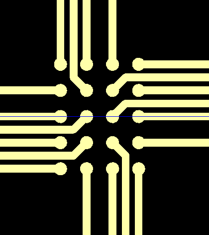
Here are the traces from the gerber files of the LRF.

The fab houses I've used all have a limit of 6mil for traces with 6mil spacing between traces.
This is what the grid looks like with 6mil traces.

Obviously 6mil traces don't leave a 6mil space between the pad and the trace.
It appears Joe Grand (who designed the LRF) used 5mil for most of the traces to the camera but these traces narrowed to 3mil when they needed to squeeze between the pads for the ball array.
The array is 0.5mm pitch.
I have not idea is I could successfully solder this part to a properly made PCB made but I'd like to give it a try.
Any suggestions on a fab house to do this kind of work?
These cameras have a tiny ball grid array on them.
Here are the traces from the gerber files of the LRF.
The fab houses I've used all have a limit of 6mil for traces with 6mil spacing between traces.
This is what the grid looks like with 6mil traces.
Obviously 6mil traces don't leave a 6mil space between the pad and the trace.
It appears Joe Grand (who designed the LRF) used 5mil for most of the traces to the camera but these traces narrowed to 3mil when they needed to squeeze between the pads for the ball array.
The array is 0.5mm pitch.
I have not idea is I could successfully solder this part to a properly made PCB made but I'd like to give it a try.
Any suggestions on a fab house to do this kind of work?


Comments
These are available from Digi-Key. These were mentioned in your thread about cell phone cameras but I don't think you were very interested since they don't produce a video signal.
I've never tried this, but you might consider adding vias in pad to go down to another layer.
-Phil
Another problem with in pad vias in this example is the minimum hole size and annular ring (of the fab houses I've used) are huge compared to this grid.
Thanks for the Advanced Circuit's suggestion SRLM. I'll see what it would cost to have them make some boards.