Shop OBEX P1 Docs P2 Docs Learn Events
Propeller 2 die picture — Parallax Forums

Propeller 2 die picture

David CarrierDavid Carrier Posts: 294
edited 2013-05-09 11:35 in Propeller 2
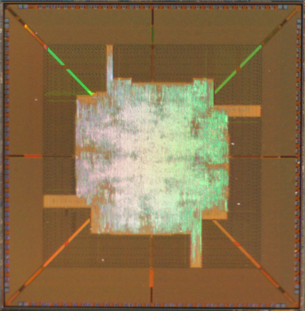
I have attached a picture of a Propeller 2 die. It is a little blurry, because I didn't have the camera's microscope adapter with me, so I ended up hand-holding it over the microscope. Fortunately the camera has image stabilization built into the body, since I wasn't using a lens.

— David Carrier
1005 x 1024 - 251K

Comments

  • W9GFOW9GFO Posts: 4,010
    edited 2013-05-06 20:15
    Cool!
    Cool!Cool!
  • jmgjmg Posts: 15,173
    edited 2013-05-06 20:22
    I have attached a picture of a Propeller 2 die.

    Are some supplied packaged, and some as bare-die ?
  • W9GFOW9GFO Posts: 4,010
    edited 2013-05-06 20:47
    I believe they received 99 packaged and 20 bare.
  • SRLMSRLM Posts: 5,045
    edited 2013-05-06 21:10
    It would be cool if Parallax made a high resolution picture of the Prop 2 die, and then printed and sold a poster.
  • pedwardpedward Posts: 1,642
    edited 2013-05-06 21:25
    For a "real" photo the top layer needs to be etched off. What your are seeing is the layer 6 poly IIRC, nothing much interesting about that layer.

    The refraction on those orthogonal lines looks neat though!
  • TubularTubular Posts: 4,702
    edited 2013-05-06 21:28
    Nice work David!
  • W9GFOW9GFO Posts: 4,010
    edited 2013-05-06 21:32
    pedward wrote: »
    For a "real" photo the top layer needs to be etched off...

    How difficult would that be to do?
  • cgraceycgracey Posts: 14,151
    edited 2013-05-06 21:41
    W9GFO wrote: »
    How difficult would that be to do?

    What's on top is the metal 6, or top metal, layer. There is glass over it, except where the pad openings are. There are 5 layers of metal under metal 6, then poly, then diffusion. You are seeing metal 6, mainly, in the picture.

    You can make out 8 clouds of metal 6 noise, arranged like pie slices in the center area. Those are the 8 cogs.

    I look at this and think, "What could possibly go wrong?"
  • W9GFOW9GFO Posts: 4,010
    edited 2013-05-06 21:53
    Would it be possible using either chemicals or temperature (or both) to weaken the bonds and separate the layers?
  • Mike GreenMike Green Posts: 23,101
    edited 2013-05-06 22:09
    @W9GFO, They're called layers, but that's not how they're made. A multilayer PCB is made in layers that are bonded together. Not so an integrated circuit. It's more like silk screening where a photo-sensitive plastic film is deposited on the surface, exposed to light in some areas and the unexposed areas washed away. Various chemicals or metal vapors are deposited in these absent unexposed areas that create the transistors or conductors, then the plastic is washed away. There are other steps that create insulating (silicon dioxide) layers and the photo-sensitive plastic film process is repeated as necessary to build other layers one at a time. There are all sorts of descriptions of these processes that you can find in the Wikipedia and elsewhere on the web.
  • W9GFOW9GFO Posts: 4,010
    edited 2013-05-06 22:27
    I had read that a layer could be an aluminum or copper film that is placed over the silicon then etched to create the wiring. I made the assumption that something similar was done for what is being called "metal 6".
  • W9GFOW9GFO Posts: 4,010
    edited 2013-05-06 22:29
    SRLM wrote: »
    It would be cool if Parallax made a high resolution picture of the Prop 2 die, and then printed and sold a poster.

    I agree, for Propeller 1 too!
  • Beau SchwabeBeau Schwabe Posts: 6,566
    edited 2013-05-06 23:40
    David,

    I have an 800x USB microscope I can bring tomorrow, and maybe get some clearer pictures.

    Attached is an example of a UVEPROM I took with the same camera.
    1024 x 768 - 59K
    1024 x 768 - 65K
  • RamonRamon Posts: 484
    edited 2013-05-07 00:05
    Please, can anyone also provide die size information?

    (to compare with propeller 1: 350nm, 7.28mm x 7.28, 53 sq mm)
  • Martin HodgeMartin Hodge Posts: 1,246
    edited 2013-05-07 00:14
    This is really cool. Thanks for posting it.
  • rjo__rjo__ Posts: 2,114
    edited 2013-05-07 09:59
    I look at this and think, "What could possibly go wrong?"

    exactly...


    I look at this and think, "Look... it's green!!!"
  • Heater.Heater. Posts: 21,230
    edited 2013-05-07 11:33
    I'm thinking, forget a picture of a real die.

    Watching Beau's presentation he was showing the design, in what ever tool that was, zooming in from the entire chip down to almost individual transistors. Panning around here and there and pulling up different layers.

    It occurs to me that a big color poster made from that actual design would be very nice.

    Just give the design tool to some suitably artistic type who can find a nice scale and color scheme.

    I mean, the shots shown here:
    http://forums.parallax.com/showthread.php/147806-Prop2-arrives-today-but-it-won-t-work?p=1182316&viewfull=1#post1182316
    are kind of fascinating.
  • potatoheadpotatohead Posts: 10,261
    edited 2013-05-07 12:41
    I found the synthesized portion fascinating. There are groups of structures piled all over the place, and that rough pie shape for the COGS is notable. You look at the human organized bits, and they are regular, orthogonal, and no where near the rats nest the synth block is.
  • Beau SchwabeBeau Schwabe Posts: 6,566
    edited 2013-05-07 16:17
    Some die pics I took with my USB microscope....

    @Ramon - The die measures 7.68mm square
    1024 x 768 - 80K
    1024 x 768 - 76K
    1024 x 768 - 50K
    1024 x 768 - 65K
    1024 x 768 - 50K
    1024 x 768 - 46K
  • TubularTubular Posts: 4,702
    edited 2013-05-07 17:05
    Can we run a poll/competition for best photo of a prop 2 die?

    I like the fourth photo, because it looks a bit like a tilt-shift small world photo. The structure looks like some kind of elaborate high tech prison designed to keep that dark maelstrom of cog logic securely held.

    I also like the third photo because the blue pin pads look very much alive
  • rjo__rjo__ Posts: 2,114
    edited 2013-05-07 18:34
    They are all beautiful... but if you make me pick.

    Beau's second picture, first post (226-2.jpeg)... looks like the P2 is reclining on a gold coin... Spanish? Piece of eight from the Otocha?


    Rich
  • localrogerlocalroger Posts: 3,451
    edited 2013-05-07 20:07
    The striking thing to me is the appearance of the logic core, which was autorouted. If you look at the P1 pictures they're very highly organized. You can sense the order there even if you have no idea what it does and it makes a pretty poster. And the outer parts of the P2 designed more by hand for the PLL's and I/O, are also very organized. But P2 logic core -- well, it's organized obviously in pizza pie fashion, but at the micro level it's sheer chaos. You ask, what was the thought process that went ... OH SNAP there wasn't a thought process, this was autorouted by a machine and WOW does it look different from the output of a human designer. I'm sure it will work and well (at least when fabbed properly *cough*) but what a mess. Turns out machines which are told to care only about efficiency don't care about symmetry or aesthetics.
  • CircuitsoftCircuitsoft Posts: 1,166
    edited 2013-05-07 20:49
    At the specific request of our esthetic guru Steve Jobs, the RAM array was spread out to match the regular grid spacing of the other chips, which didn’t work out so well: the increased trace lengths caused a troublesome increase in noise on the high-speed RAM signals, so the next board went back to the more densely packed array.
    Macintosh Prototypes
  • LawsonLawson Posts: 870
    edited 2013-05-07 20:54
    Some die pics I took with my USB microscope....

    @Ramon - The die measures 7.68mm square

    Hm... lots of .jpeg smearing. Is that the forum software or the microscope? If you have a digital camera with a long zoom lens, a strong hand magnifying glass is enough to do some nifty macro work. I've been able to get a whole almond to fill the picture frame that way. It's such a pretty die, I want to see more detail!

    Lawson

    P.S. whoever mentioned making the layout view a poster has an awesome idea. Some re-colored layouts from a side project of mine.
  • Beau SchwabeBeau Schwabe Posts: 6,566
    edited 2013-05-07 21:42
    @Lawson - Some of that smearing is a moire effect due to the slotting in the top metal. You don't see the slots, but you see some of the effect of the slots. If you look close on some of the images, you can see a 'ghost' under the top metal. If the slots weren't there you wouldn't see the image below at all. When the top metal reaches the infamous "Core perimeter" , the top metal turns into something that resembles a wire screen on a window, except every other wire on the screen is Power and Ground. This allows you to 'see' a lot more of the other layers, making it look like a 'cloud'

    @localroger - The automated spaghetti routing is a result of precise timing that would otherwise be incredibly difficult or near impossible to do by hand. If you can visualize the Propeller I with COGS on top and communication buss on the bottom. Take the East and West most ends and wrap them together so that it forms a circle (COG0 would abut COG7) with the communication buss now located in the center. That essentially is how the auto-router placed the design together, resulting in the 8 'lobes' you see representing each cog. Using a central communication buss between COGS was essential in meeting communication timing requirements.


    I like the idea of a poster ... let's get the P2 corrected and worry about that stuff at a later time.
  • KeithEKeithE Posts: 957
    edited 2013-05-09 11:35
    Do you have the equipment to take an IR picture from the bottom?

    Edited to add: in case the intent of this was misunderstood, even with an unpowered die you would see structures. From wikipedia - "Silicon is transparent to infrared light with wavelengths above about 1.1 micrometres." Not as pretty as some pics, but it's an easy thing to do. I went through this with both powered and unpowered chips (WLBGA package) at EAG when we had a static RAM going into a high-power state.
Sign In or Register to comment.