Shop OBEX P1 Docs P2 Docs Learn Events
My First ExpressPCB order... help review please! — Parallax Forums

My First ExpressPCB order... help review please!

doggiedocdoggiedoc Posts: 2,239
edited 2013-01-04 18:37 in General Discussion
.

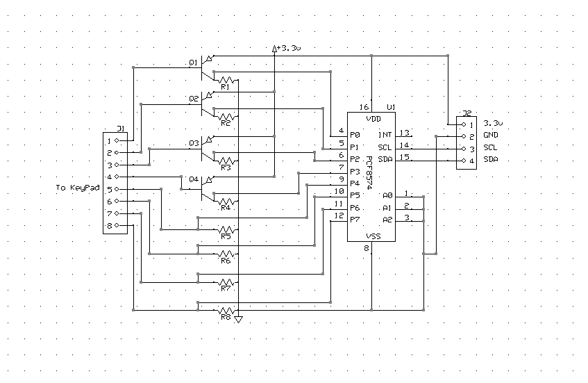
If you remember a while back I was working on a Keypad Decoder, the Hard Way. Well thanks for all the help then. Especially Beau Schwabe for the simplification of the design. Well with some time on my hands for the Holidays, I finally got around to laying out a PCB and it has taken me a day or two to get to this point. :D

I added an 8 bit I/O expander to reduced the Pin usage to just 2 pins. I'm pleased with the result now and think I am ready to order prototype boards.

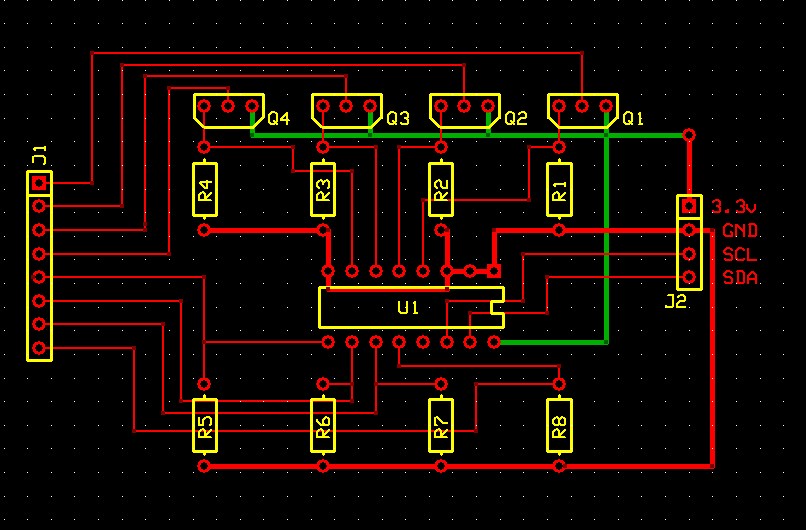
Here are the Schematic and PCB images. Please advise on what I may have screwed up or could maybe could have done better.

Thanks!

Paul

Schematic:

4x4_keypad_decoder_SCH.png


PCB:

4x4_keypad_decoder_PCB.png
«1

Comments

  • Duane DegnDuane Degn Posts: 10,588
    edited 2012-12-24 15:53
    Most of my PCB layout knowledge comes from reading the forum. I've had very few actual PCBs made so I'm just spouting what I've heard here.

    Apparently right angles are looked down on for PBC layouts. They can cause problems with high speed signals and I've been told they don't etch as well as 45 degree angle turns.

    The way the traces meet the holes for R2 and R3 aren't dead on. Again, I've been told these can cause etch problems (acid traps is what I've been told).

    Hopefully someone with really experience will chime in.
  • doggiedocdoggiedoc Posts: 2,239
    edited 2012-12-24 16:17
    Cool! That's the kind of advice I was looking for!
  • doggiedocdoggiedoc Posts: 2,239
    edited 2012-12-24 17:02
    I've taken all the right angles out that I can. The power trace on the bottom layer that runs under Q1 thru Q4 - I'm not sure how to do those....


    4x4_keypad_decoder_PCB_2.png
  • SRLMSRLM Posts: 5,045
    edited 2012-12-24 17:08
    Thin traces are worse than big traces: you should make them bigger.
  • doggiedocdoggiedoc Posts: 2,239
    edited 2012-12-24 17:18
    SRLM wrote: »
    Thin traces are worse than big traces: you should make them bigger.
    All of them or just the ones's I can't fix the right angles on?

    And thanks for the tips!

    :D
  • doggiedocdoggiedoc Posts: 2,239
    edited 2012-12-24 17:35
    SRLM wrote: »
    Thin traces are worse than big traces: you should make them bigger.
    How's this?

    4x4_keypad_decoder_PCB_3.png
  • Mark_TMark_T Posts: 1,981
    edited 2012-12-24 17:42
    Groundplane?

    Decoupling capacitor(s)?


    The right-angle thing matters for GHz speeds on stripline, less important at lower speeds, but 45 deg angles look
    much more professional ;)

    Thin traces fine for logic - reduces crosstalk in fact when over a groundplane. thick traces for supply between
    chips and decoupling capacitors at least.
  • ElectricAyeElectricAye Posts: 4,561
    edited 2012-12-24 18:27
    It might be good experience for you to try a ground plane instead of using traces going back to the GND. Ground planes help to reduce signal interference, and you might find they are very useful some day when working with more sensitive circuits. Consider the "thermal pad" option when connecting your resistors, etc. to the ground plane, and that will help make it easier for you to solder the resistor leads to the ground plane. If you chose "solid pad", you might find that the ground plane sucks away too much heat from your soldering iron, and thus those solder points will be difficult. If you've got extra space on your PCB, consider putting the date and some other ID on it so you'll know what the board is 3 years from now (when you've boxes full of such boards and they're all the same size and you haven't got a clue).
  • doggiedocdoggiedoc Posts: 2,239
    edited 2012-12-24 19:18
    It might be good experience for you to try a ground plane instead of using traces going back to the GND. Ground planes help to reduce signal interference, and you might find they are very useful some day when working with more sensitive circuits. Consider the "thermal pad" option when connecting your resistors, etc. to the ground plane, and that will help make it easier for you to solder the resistor leads to the ground plane. If you chose "solid pad", you might find that the ground plane sucks away too much heat from your soldering iron, and thus those solder points will be difficult. If you've got extra space on your PCB, consider putting the date and some other ID on it so you'll know what the board is 3 years from now (when you've boxes full of such boards and they're all the same size and you haven't got a clue).

    Thanks for the tips!

    Here's a new version:
    4x4_keypad_decoder_PCB_4.png
  • frank freedmanfrank freedman Posts: 1,982
    edited 2012-12-24 19:38
    Go wider trace on 3.3v, and the end run to q4 could be 45 degree. I haven't done a board since mid '80s (bishop pads and tape jobs), but it may be worth leaving as much copper on the red side as well. Uses less etchant. Problem with 90 degree turns is loosing trace width from etching under a little on the pointy side but long time back, could be wrong on that.

    FF
  • doggiedocdoggiedoc Posts: 2,239
    edited 2012-12-24 21:00
    Go wider trace on 3.3v, and the end run to q4 could be 45 degree. I haven't done a board since mid '80s (bishop pads and tape jobs), but it may be worth leaving as much copper on the red side as well. Uses less etchant. Problem with 90 degree turns is loosing trace width from etching under a little on the pointy side but long time back, could be wrong on that.

    FF
    Thanks Frank! This will be my last revision for the night! Merry Christmas!! Thank you al for the help thus far!

    4x4_keypad_decoder_PCB_5.png
  • doggiedocdoggiedoc Posts: 2,239
    edited 2012-12-24 21:03
    Smile.... I forgot the pull up resistors on SDA and SCL. Guess I'll work on that tomorrow!

    Thanks everyone!

    Paul
  • doggiedocdoggiedoc Posts: 2,239
    edited 2012-12-24 21:33
    I couldn't stand it! I had to add the pull-ups! -- Now I can go to sleep! Merry Christmas!

    4x4_keypad_decoder_PCB_6.png
  • SRLMSRLM Posts: 5,045
    edited 2012-12-24 22:29
    If you're going to use a ground plane, you have to use one on both sides of the board. You want to make sure that the amount of copper on both sides of the board matches, otherwise the board may warp.

    It looks like you can also make this a one layer board by routing between the pins of the IC. This is a choice of yours, but I would prefer minimizing the number of layers.

    You might also want to consider adding mounting holes, along with the previously mentioned informational text.

    You can make the board smaller (and, hence, possibly cheaper) by moving R5-R8 up to a more compact position.
  • doggiedocdoggiedoc Posts: 2,239
    edited 2012-12-24 22:56
    Thanks for the tips! One more revision.... the kids will be up soon! Santa is tired!

    4x4_keypad_decoder_PCB_7.png
  • SRLMSRLM Posts: 5,045
    edited 2012-12-24 23:20
    I'd also move the R6 red trace back to the top layer of the board, since you have plenty of routing room. You could make the board even smaller by moving those bottom resistors up, and running some traces underneath the resistors, but it's not necessary if you don't need to make you board as small as possible.
  • frank freedmanfrank freedman Posts: 1,982
    edited 2012-12-24 23:38
    If you rotate the transistors 90 d ccw, you could move the 3.3v trace to the bottom layer. Also route the power to the ic around the board edge of the connector and keep the supply entirely on the bottom side of the board. Finally if you re-route pin 10 to the resistor and from there to the J1 connector under R5 then you will have succeeded in creating a single sided board. Also, you may want to add a .1uF cap near the ic for decoupling and perhaps a small electrolytic 10uF or so for filtering.

    If you really want to shrink the thing, go surface mount. Transistors and 0612 format resistors and caps are easy to do with fine tip. Also the ic may be available in soic so even that is doable without much effort. Possibly reduce the cost with fewer through holes to drill/plate etc.
  • Mark_TMark_T Posts: 1,981
    edited 2012-12-25 02:25
    Also, you may want to add a .1uF cap near the ic for decoupling and perhaps a small electrolytic 10uF or so for filtering.

    Surely that's "you must add 0.1uF decoupling cap next to the IC". No logic chips are guaranteed to work (reliably) without proper supply decoupling.
  • BeanBean Posts: 8,129
    edited 2012-12-25 04:55
    You don't need the via for the trace coming from J1.6
    Just run that top trace all the way to the IC pin on the top side.

    And as others have pointed out, get a decoupling cap on that IC.

    Bean
  • ElectricAyeElectricAye Posts: 4,561
    edited 2012-12-25 07:31
    Just remember that the yellow lettering, which you used for your identification, will only show up on the PCB if you order it that way. If you're using the company's cheap mini-board service or whatever it's called, then you won't get that lettering unless you pay extra. You can have your identifying info show up in copper if you want, and that saves a little money.

    Also, when using ground planes, keep an eye on the width of the copper plane between traces, such as you have above your parts labeled Q's. For example, if you were to expand the width of those traces, there's a possibility of the copper plane between those traces getting unacceptably thin, which could cause the ground plane there to peel off and cause shorts. I don't think you're in any danger of that now, but it's just something to watch out for if you make changes.

    Merry Christmas, Santa
  • doggiedocdoggiedoc Posts: 2,239
    edited 2012-12-25 09:12
    Thanks all - I added a decoupling cap to the VDD of the IC, removed the via and rerouted the trace from j1.6 and moved it to the bottom layer, repositioned R5 and R6.

    A couple of you have mentioned making the board smaller to save cost - the ExpressPCB mini board service is a fixed size for a flat rate - so I've got room to spare on this one.

    Here's the latest improvements you all have so graciously helped with.

    4x4_keypad_decoder_PCB_8.png
  • SRLMSRLM Posts: 5,045
    edited 2012-12-25 14:24
    Don't forget the bottom copper pour.
  • frank freedmanfrank freedman Posts: 1,982
    edited 2012-12-25 14:31
    @ Mark, my design is one per chip always. When suggesting to another consider "you may want to xxx" as very strong recommendation. Since my stuff is one off, overkill is good and saves me time not spent chasing ghosts an intermittents.
    Mark_T wrote: »
    Surely that's "you must add 0.1uF decoupling cap next to the IC". No logic chips are guaranteed to work (reliably) without proper supply decoupling.
  • frank freedmanfrank freedman Posts: 1,982
    edited 2012-12-25 14:46
    Pull J2 in a bit and rotate the transistors. Might need a bit of trickery routing the trace. Then you should be able to route the 3v supply on the same side as the rest of the runs for a single sided board. Not sure if you missed that earlier or decided to leave well enough alone......
    doggiedoc wrote: »
    Thanks all - I added a decoupling cap to the. VDD of the IC, removed the via and rerouted the trace from j1.6 and moved it to the bottom layer, repositioned R5 and R6.

    A couple of you have mentioned making the board smaller to save cost - the ExpressPCB mini board service is a fixed size for a flat rate - so I've got room to spare on this one.

    Here's the latest improvements you all have so graciously helped with.

    4x4_keypad_decoder_PCB_8.png
  • frank freedmanfrank freedman Posts: 1,982
    edited 2012-12-25 14:58
    Sorry to annoy with more afterthoughts, but you could also use resistor arrays for r 1-4 and r 5-8 with the same spacing as the ic pin spacing plus the common point to gnd. Simplify the layout further that way.
  • localrogerlocalroger Posts: 3,451
    edited 2012-12-25 16:45
    doggiedoc, I wouldn't bother with the ground plane unless you're doing real RF stuff. I've done many, many ExpressPCB boards. It's much more important to use thick traces when possible. The problem with right angles is that with thin traces the etchant can burrow under the mask compromising the copper width. With thicker traces 90 angles are less of a problem, although I avoid them out of habit. Unless you're getting an advanced service with solder mask and/or laying out a VHF transmitter, ground planes are likely to cause much more trouble than they cure.
  • electromanjelectromanj Posts: 270
    edited 2012-12-25 19:29
    Hi Paul,Great looking board! Not sure if this was already mentioned but, if you are using the miniboard service that doesn't include silkscreen or soldermask, you can still include the board name and header lables by moving them to the top or bottom copper layer.
    traVis.
  • doggiedocdoggiedoc Posts: 2,239
    edited 2012-12-25 19:41
    Thanks Travis! Merry Christmas!
  • ElectricAyeElectricAye Posts: 4,561
    edited 2012-12-25 19:50
    localroger wrote: »
    doggiedoc, I wouldn't bother with the ground plane unless you're doing real RF stuff. ....

    I would think having a ground plane helps to protect a non-RF circuit board from interference from the environment, at least somewhat. I seem to remember a circuit I had with a real time clock (RTC) getting reset due to a device in the same room that would do some fancy inductive loading now and then. The addition of a ground plane seemed to solve the problem, and since then, I've been using ground planes as an RFI preventative measure for many of my circuits. Have I been wasting my time with ground planes? Do they not help in holding down some RFI? Hey, if nothing else, shiny ground planes look better than those dull boards you get with the miniboard option. Adding a ground plane makes the PCB look like you almost know what you're doing sometimes. No?
  • doggiedocdoggiedoc Posts: 2,239
    edited 2012-12-26 05:34
    I can't thank you all enough for the input. ElectricAye - at the moment I've taken the ground plane off because it makes it hard for me to 'proof read' the trace connections. Last night I had a what if moment and decided I needed a parallel output option too. Here is the Revision B schematic:

    4x4_keypad_decoder_SCH_RevB.png
Sign In or Register to comment.