I keep painting my self in to a corner
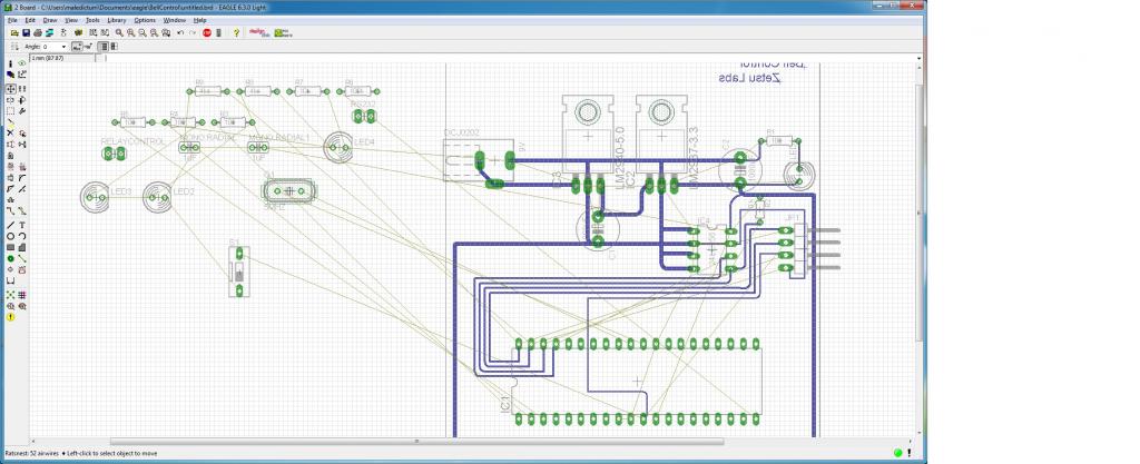
I am trying to layout a pcb and its going terrible... I get 3/4 the way done and find i have painted a part into a corner ( cant hit + power rail on my pcb without crossing - ). Anyone have tips suggestions on doing this. ( currently I am just laying out parts how I would think they would best fit then attempting to connect them up.
First thing i did was layout the Power supply on the board (including traces), then attempted to add in the EEprom, and the prop (including traces), then add in the extras...
I never make it past phase two....
I would of attached the actually eagle files, but I am not where I can access them.
Also is it wise to run traces so close to pads as I have done in some areas ???


Comments
I have been thinking about that for a while, Or if i could find boards that are double sided that work with Photo Resist etching. Now I know how one of those rats in a maze feels like, just I have the ability to move around walls...
You first few boards are going to be ugly and may have some surprises. Exactly how close to pads are you running wires? I sometimes run the wires between the pads and it works okay.
A double sided photo-resist board can be found, but it is tricky to get both sides lined up. I expose one side. Then drill holes for a couple of items in opposite corners and then have to match those drilled holes to the transparency when I expose the other side.
I suppose one could make sure two adjacent edges were perfect and do it that way. But you might as well save your money and learn the first few on single sided boards.
I also suggest that you try an autorouter such as Freerouter. This will tell you if it is even possible to route your board.
Lawson
When designing the circuit take the layout into account when selecting the chips.
For example the 74HC240 octal buffer has 4 inputs and 4 outputs on each side of the chip while the functionally equivalent 74HC540 has all the inputs on one side and the outputs on the other side. The same is true for some of the other 5xx chips. Makes layout much simpler at times.
Use a wire jumper for the negative and positive supply that can also be used as a test point for debugging/troubleshooting the circuit by putting a loop in the jumper wire.
The same can be done for signals, so select signals to be jumpered with this in mind whenever possible.
- Place your components first
- Click on the Auto button
- Under the General tab, sub-item Top, select N/A, and for Bottom, try different settings. One may be successful.
- Additionally, if all the Bottom settings are unsuccessful, go to the DRC, and try altering the clearances, this could change everything.
EDIT: After placing the components, hit the Ratsnest button, which should show you obviously wierd placements. Rearrange obvious blunders, perhaps just rotating a few parts.http://forums.parallax.com/showthread.php?143250-Basic-Propeller-circuit-on-a-proto-board
I often try an up-the-middle approach. Or try to have a separate island for voltage regulation and the rest for whatever the ICs force me to do.
The second side is used as a ground plane.
This ground plane often greatly simplifies the signal side by getting rid of the pesky ground foils.
Besides, the solid ground plane is much superior in terms of supply noise.
Note!! After drilling all the holes a "Chamfer" bit, a little larger drill bit, is used to remove the copper around holes where the pins are not to be connected to the ground plane.
Another trick is to convert DIP packages to gull wing for surface mount soldering. The few pins that do use ground are left strait and go through to the ground plane on the bottom side.
Duane J
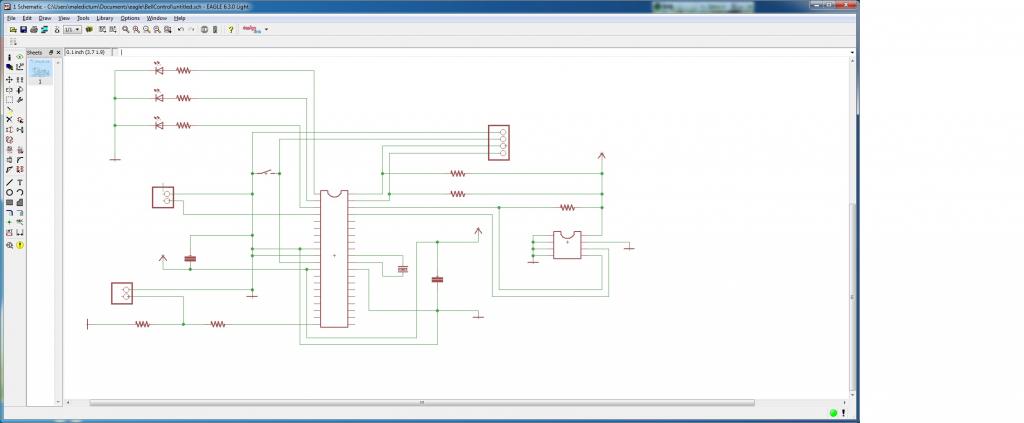
The traces from Pins 30 and 31 going to the four pin header have two resistors branching off and going to ground. Why do you have these resistors?
Bruce
AMEN ! .. its the only way I make my home brew stuff..
Peter..
It's probably for the FTDI reset issue: http://forums.parallax.com/showthread.php?116711-Can-Parallax-do-something-about-the-FTDI-reset-bug (ps: I think they are pull ups, not pull downs)
-Phil
I used to do the gull wing thing but it never crossed my mind to leave the ground pin(s) as suggested. Brilliant in it's simplicity. Thanks Duane.
@Phil
In the thread that SLRM referenced, I now see your advice:
EDIT: I am glad I asked that question, and thanks for the responses. Now I have to break out the crowbar and fix one of my schematics and layout.
I think that's eagle doing something strange...
I have some resistors ( they should be pull ups) that are on the sda and i think its called the sdl lines ? for the i2c circuit. Its preventing the prop from power cycling, when a computer isn't plugged into the usb-plug. Unless You are talking about something else and I just didn't see what you meant.
It is a Propeller I just have not finished the PCB layout to show the coupling across the chip.