Laugh At It If You Must, Critique It If You Must, But I Think It'll Do The Trick :)
 idbruce
Posts: 6,197
Hello Everyone
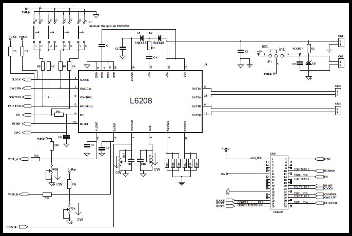
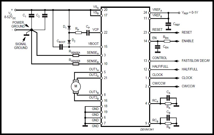
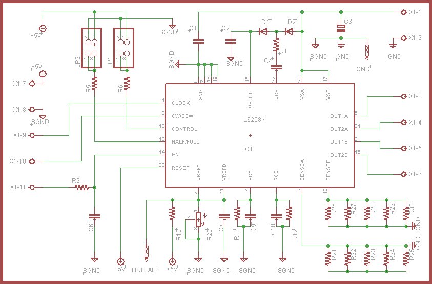
Over the last several days, I have been combining the schematic of the EVAL6208N and the typical application schematic for the L6208N stepper driver IC, and I have a very good idea just how I want the board laid out. I know this is no big deal for some of you, but for me, it was a bit time consuming. Although I am not 100% certain, I do believe this design for a stepper driver should be good enough for my first trial. And yes I know, I jumped some numbers in the part naming, but I will fix that when I get a very accurate list of the actual part numbers. If you see any blatant errors, please let me know.
Bruce
EDIT: ERROR FOUND!!! Please refer to Post #6.


Comments
LOL You got a chuckle out of me.
I definitely plan to use the ground plane as a heat sink, so I surely appreciate the tip, and I will have to do some research on a good remedy for the problem that you describe. The EVAL6208N claims to be able to withstand 2.86A and it uses nothing more than the ground plane for the heatsink, so I believe I can accomplish the same by following the EVAL6208N grounding layout. I used fans on some other driver boards I made and it caused me a lot of extra work. I also intend to try and achieve that 2.86A benchmark, and if I release some magic smoke, I guess I will know better next time.
Bruce
[edit: you need to use NORMAL MODE for microstepping this way, both phases driven]
Yea I know, but I decided to just do half and full steps this time around, just to get me feet wet with this chip and test the amperage rating of the board without fans or a heatsink. If all goes well, I might try a microstepping board or perhaps try and progress to the L6480H. Anyhow thanks for the corcern, I appreciate it.
Bruce
Bruce
Fifty percent of this board is modeled after the EVAL6208N evaluation board, so alot of my layout was dependent upon that schematic and layout of that board. If you look at the attached images, you will see that the main ground plane is on the top layer and that there are alot of traces on the bottom layer. I would imagine that the chip is placed in direct contact with the top layer for heat dissipation purposes.
Bruce
In order to assist with the visualization of the similarities between my board and the EVAL6208N, I have attached two more images which only show the component layers for both boards.
Bruce
Before getting too carried away with my current project, I decided to review the necessary components, values, and initial layout. The desire to create a PCB design around the L6208N actually started several years ago. In fact as previously mentioned, I already designed one board around this chip, but I was very unhappy with results. One of the problems that I had way back then was finding a suitable substitute for the sensing resistors. With the substitution resistors that I am currently using, this choice of resistors has increased the board length by an unnecessary amount 3/8 - 1/2". Considering that my biggest concern is the size of the board, which is currently 3.35 X 2.75", I believe I will revisit the issue of the components and values for the sensing resistors. If I can find more suitable replacements for the sensing resistors, this should result in a board size of approximately 2.75 X 2.75", however I will have to alter the design and rearrange the layout a little to compensate for these changes.
Bruce
I will be looking for (6) 1 Ohm, 0.4Watt, metallic film resistors per board. If I can find them, I should be able to modify my current design with minimum hassle, and shrink the board considerably. I have not looked for them in approximately 3-4 years, but I should be able to find something compatible. If necessary, I could perhaps increase the power rating to 1/2W, which would make my search easier, but I would have to review the datasheet to see if that combination will work properly.
Bruce
I would have to redesign my whole board to compensate for surface mount resistors and I am not prepared to do that. I think I will stick with my current design of the board and use these resistors or similar resistors of the same series:
Bruce
I rearranged quite a few things, and with the exception of drawing my various planes and rearranging a few part names, I believe this baby is ready for production. The board will measure 2.70" Wide X 3.00" Long. Oh, and I am shooting for 2.5A per phase.
Bruce
EDIT: I just realized that I forgot to add a power LED. Oh well, that is pretty much just show anyhow.
On the half/full jumper, why do you have two? Put a large pullup on it, and have the jumper pull it low. That way, you won't have an illegal condition if somebody either forgets the jumper or puts two on. Same with the fast/slow decay switch.
As mentioned, a large portion of this board is modeled after the EVAL6208N. If you refer to Post #9, which shows the top and bottom layers for that board, you will see that the whole sensing area is comprised of three planes, which will rectify the thin traces going from the chip to the sensing resistors. Additionally, the positive and the negative of the main filter capacitor is also attached to two major planes, which would also rectify those thin traces.
Thanks for pointing that out to me, because that is a serious potential problem. By placing two jumpers or a single jumper across the wrong two terminals, a direct short would exist.
Thanks for the advice.
Bruce
I do believe I need a little help.
As can be seen on my board in Post # 18, JP2 is goes to one side of R3 and the other side of R3 goes to PIN 12 (HALF/FULL) of the L6208N. Additionally R3 has a resistance of 10K Ohms. The default for the drive is FULL step mode, with a jumper positioned on JP2 so that GND is going to R3. In HALF step mode, a jumper would be positioned on JP2 so that 5V is going to R3, instead of GND going to R3. In the original schematic and on the EVAL6208N evaluation board, STMicroelectronics had the exact same circuitry, except they used a two position switch to make and break contact between GND and 5V. However as Circuitsoft so kindly pointed out in Post #19, a direct short could occur if someone placed a jumper in the wrong position. Now we all know this would never happen to me
By examining the board layout in Post #18, you will see exactly what he is talking about, and as he mentions, there are two identical problem areas, but they should both have the same solution. Even though he definitely has the right idea, I want to switch his solution around a little to provide the default settings without jumpers, as it applies to the EVAL6208N evaluation board schematic. In order to do this, although not 100% certain, I believe that I would need to use a pull down instead of a pull up. I base this upon the datasheet which says:
The attached image below depicts the proposed solution, however I am uncertain how to obtain the proper values for R3 and R_UNKNOWN. Considering the original value of R3 (10K), how would I determine the new value of R3 and the value for R_UNKNOWN?
Thanks in advance.
Bruce
For those that may be interested, I have attached three more images to show the current state of everything. Please note that you may copy my work and layout for personal use, but commercial use is out of bounds.
Bruce
I just got finished with the copper pours/planes (whatever you want to call them) for the bottom layer. I have attached an image of my bottom layer and the bottom layer of the original EVAL6208N evaluation board, so that you can compare them and notice some of the similarities.
Bruce