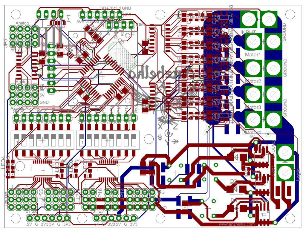
UPDATED: PCB Board Review (Quadrotor) v2
[size=+2]Updated board revision![/size]
For my capstone engineering project I am working on developing software to control a quadrotor UAV with another student (he's not a regular forum member, but he may pop in). We have designed our own PCB to be the basic control board and are looking for feedback on the design of the board, and any manufacturing issues that we may run into.
The board consists of two main features: a power distribution area to take incoming battery connections and send that to the appropriate areas, and the Propeller based control circuits necessary to a simple flight controller. More details are in the following post.
Some general notes:
1. Nearly all components are topside. A few power resistors are on the bottom.
2. We tried to make the board very flexible without sacrificing reliability or functionality.
3. Most chips have decoupling capacitors added in order to provide stability

[size=+2]UPDATE: New board revision, any last comments or things that we missed?[/size]
[size=+1]PDF attachment contains different views of the board and full schematics.[/size]
Specific Questions:
Q1. Should we add copper pours to the left over open spaces, and if so do they need to be connected to ground? A: Yes, we should
Q2. Does it matter that the four SD card IO pins (SPI + CD) are routed under the Propeller? Moved the routing
Q3. Can traces go underneath the edges of the crystal (the area not between the crystal pins)
Q4. Would it be better to have the spare ADC on the right (8 analog lines routed under and around Propeller) or on the left (3 IO lines, including SPI CLK routed under or around the Propeller). Moved it
Q5. Is there a better layout for components that can improve routing? It looks like a rat's nest to me, but is that normal?
Q6. Is there anything that you think needs to be done?
For my capstone engineering project I am working on developing software to control a quadrotor UAV with another student (he's not a regular forum member, but he may pop in). We have designed our own PCB to be the basic control board and are looking for feedback on the design of the board, and any manufacturing issues that we may run into.
The board consists of two main features: a power distribution area to take incoming battery connections and send that to the appropriate areas, and the Propeller based control circuits necessary to a simple flight controller. More details are in the following post.
Some general notes:
1. Nearly all components are topside. A few power resistors are on the bottom.
2. We tried to make the board very flexible without sacrificing reliability or functionality.
3. Most chips have decoupling capacitors added in order to provide stability
[size=+2]UPDATE: New board revision, any last comments or things that we missed?[/size]
[size=+1]PDF attachment contains different views of the board and full schematics.[/size]
Specific Questions:
Q1. Should we add copper pours to the left over open spaces, and if so do they need to be connected to ground? A: Yes, we should
Q2. Does it matter that the four SD card IO pins (SPI + CD) are routed under the Propeller? Moved the routing
Q3. Can traces go underneath the edges of the crystal (the area not between the crystal pins)
Q4. Would it be better to have the spare ADC on the right (8 analog lines routed under and around Propeller) or on the left (3 IO lines, including SPI CLK routed under or around the Propeller). Moved it
Q5. Is there a better layout for components that can improve routing? It looks like a rat's nest to me, but is that normal?
Q6. Is there anything that you think needs to be done?


Comments
4. Motor and servo battery is connected via a Deans plug at the top position, and four Deans plugs for the ESCs below that.
---a) Each ESC has a voltage and current measurement circuit (top four blocks of red components on the right hand side)
5. Logic battery connection is the bottom most Deans plug (green, bottom right), and it powers the 5v and 3.3v logic circuits. An additional 5v circuit is powered by the motor battery for servos.
---a) Voltage and current is also measured for the servo 5v circuit, the logic battery draw, and the 5v and 3.3v logic circuits (next four red blocks on the right hand side)
Control Circuits:
6. The Propeller is meant to be overclocked, and so has capacitors on three of it's 4 VDD/VSS pairs. The fourth we decided to not put a capacitor on in order to allow the crystal to be as close as possible.
7. Three MCP3208s powered at 5v are used to provide ADC. Two are used to measure the voltages and currents of the power distribution area, and the third is broken out to a header on the left hand side (with 5v, GND, and ADC in on the three pin header)
8. Two TXB0108PW logic level shifting chips are used to provide level shifting for ESCs and servos. These are on the bottom left of the board. Each also has a bank of switches on the 3.3v side, and a set of headers. This is to allow a specific IO line to be disabled and used for something else. We have provided LEDs on two in the anticipation of using these for TX/RX wireless communication.
9. Headers for the following:
---- PWM
Servos, grouped into blocks of 2, 2, and 4
ESCs, grouped into a block of 4 (without a connection on the center pin)
ADCs (5v circuit), grouped into 2 blocks of 2
I2C (in a header with 3.3v and GND)
SD card (in the same order as Parallax's SD card and uSD card breakout boards).
GPIO pins, either at 3.3v or 5v. Two have LEDs attached (4 available)
Power, in groups of (3.3v, GND, 5v). 4 groups.
CHR-6 IMU (5v, GND, IO, IO).
Propeller Plug (standard)
Deans plug headers for Batteries and ESCs
10. Mounting holes as follows:
Board mounting holes to fit Parallax BOE standard.
Additional mounting holes to stack Quickstart boards.
Holes for the CHR-6 IMU plain PCB board.
Holes for a Parallax SD card breakout board (rotated a bit to fit, over the bottom left hand side of the board.
Errata (things we know about): Updated
11. The prop plug header soldermask is facing the wrong way. It should be pointed up.
12. Some of the soldermask stuff overlaps. We'll get that fixed...
13. The soldermask label ESC and Unused (on the PWM output on bottom) should be switched.
For applications that generate heat and uses the pcb copper to get rid off it
I make both sides copper pours that is the gnd (Vss) net.
And place a few vias around the heat sources to channel some of it to the bottom copper.
Your PCB layout is a little hard on the eyes, but if it works.
Here is an example, though not the best as it's soo tiny that it's not much empty space left for pour.
Lilly=39x22mm p0-p7 brough out, usb chip, eeprom, r/c dac, dual sigma adc, both video and vga, dual h-bridge/stepper
but more about her later when I have one populated.
Any further comments on our design?