

2.4" LCD Touchscreen. Getting the screen to come on and do something, anything?
 eagletalontim
Posts: 1,399
eagletalontim
Posts: 1,399
Well, I am back at it again and this time with something that is way out of my abilities. I have purchased 2 each 2.4" LCD touchscreens from here :
http://iteadstudio.com/store/index.php?main_page=product_info&cPath=57_58&products_id=55
I have been following these 2 posts which are also working with touchscreens :
Thread 1: http://forums.parallax.com/showthread.php?137266-Propeller-GUI-touchscreen-and-full-color-display > Using the same screen as I am but using latches instead of direct connections to the Prop as I am doing.
Thread 2: http://forums.parallax.com/showthread.php?137999-LCD-touchscreen-A-development-thread > Using a different display, but not using latches. Similar code as well.
What I have done so far is wired up my display exactly like done in Thread 2. I am using the screen initialization method in Thread 1 since it is for my screen. I have attached the testing file that I have modified for my setup from Thread 2. When the Prop is powered on, the LCD backlight comes on instantly but after that, nothing changes on the screen. I have temporarily connected LED's to each pin that controls the screen and some of them flash the LED about 1 second after power is connected so I know the program is running and the screen is receiving the signal. I have also tried 2 different screens with no change with either screen.
Here is the pinout of the LCD :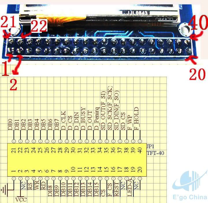
Do I have something wrong?

Comments
That would indeed be a bad idea! Yes, you need caps for running anything reliably on the prop. There are severals threads discussing capacitor issues.
If that is the code as it is, it will run the Start method but it still needs to run the Draw method and the Pixel method from somewhere.
Also a photo of the board would be helpful if there is some discussion about capacitors being left out.
If the code I posted is close, could someone help me get it farther than that? I don't have a way to take a picture and upload it at the moment. I am not even sure a picture will help since my circuit looks like a spider sitting on top of the 40 pin Prop.
PUB Start_SSD1289
    ''init pins
    OUTA[SD_CS] := 1
    OUTA[TS_CS] := 1
    EnableDisplayPins                                     ' enable pins 0 to 15

    ResetHigh
    wait.pause1ms(5)

    ResetLow
    wait.pause1ms(5)
    ResetHigh

    WriteHigh
    wait.pause1ms(5)

    Lcd_Write_Com($00,$E5)
    Lcd_Write_Data($78,$F0)                               ' set SRAM internal timing
    Lcd_Write_Com($00,$01)
    Lcd_Write_Data($01,$00)                             ' set SS and SM bit
    Lcd_Write_Com($00,$02)
    Lcd_Write_Data($07,$00)                             ' set 1 line inversion
    Lcd_Write_Com($00,$03)
    Lcd_Write_Data($10,$30)                             ' set GRAM write direction and BGR=1.
    Lcd_Write_Com($00,$04)
    Lcd_Write_Data($00,$00)                             ' Resize register
    Lcd_Write_Com($00,$08)
    Lcd_Write_Data($02,$07)                             ' set the back porch and front porch
    Lcd_Write_Com($00,$09)
    Lcd_Write_Data($00,$00)                             ' set non-display area refresh cycle ISC[3:0]
    Lcd_Write_Com($00,$0A)
    Lcd_Write_Data($00,$00)                             ' FMARK function
    Lcd_Write_Com($00,$0C)
    Lcd_Write_Data($00,$00)                             ' RGB interface setting
    Lcd_Write_Com($00,$0D)
    Lcd_Write_Data($00,$00)                             ' Frame marker Position
    Lcd_Write_Com($00,$0F)
    Lcd_Write_Data($00,$00)                             ' RGB interface polarity
'        *************Power On sequence ****************//
    Lcd_Write_Com($00,$10)
    Lcd_Write_Data($00,$00)                             ' SAP, BT[3:0], AP, DSTB, SLP, STB
    Lcd_Write_Com($00,$11)
    Lcd_Write_Data($00,$07)                             ' DC1[2:0], DC0[2:0], VC[2:0]
    Lcd_Write_Com($00,$12)
    Lcd_Write_Data($00,$00)                             ' VREG1OUT voltage
    Lcd_Write_Com($00,$13)
    Lcd_Write_Data($00,$00)                             ' VDV[4:0] for VCOM amplitude
    Lcd_Write_Com($00,$07)
    Lcd_Write_Data($00,$01)
    wait.pause1ms(50)                                  ' Dis-charge capacitor power voltage
    Lcd_Write_Com($00,$10)
    Lcd_Write_Data($10,$90)                             ' 1490//SAP, BT[3:0], AP, DSTB, SLP, STB
    Lcd_Write_Com($00,$11)
    Lcd_Write_Data($02,$27)                             ' DC1[2:0], DC0[2:0], VC[2:0]
    wait.pause1ms(50)                                  ' delay
    Lcd_Write_Com($00,$12)
    Lcd_Write_Data($00,$1F)                             '001C// Internal reference voltage= Vci;
    wait.pause1ms(50)                                  ' delay
    Lcd_Write_Com($00,$13)
    Lcd_Write_Data($15,$00)                             '$1000//1400   Set VDV[4:0] for VCOM amplitude  1A00
    Lcd_Write_Com($00,$29)
    Lcd_Write_Data($00,$27)                             '$0012 //001a  Set VCM[5:0] for VCOMH  //$0025  0034
    Lcd_Write_Com($00,$2B)
    Lcd_Write_Data($00,$0D)                             ' Set Frame Rate   000C
    wait.pause1ms(50)                                  ' delay
    Lcd_Write_Com($00,$20)
    Lcd_Write_Data($00,$00)                             ' GRAM horizontal Address
    Lcd_Write_Com($00,$21)
    Lcd_Write_Data($00,$00)                             ' GRAM Vertical Address
'         ----------- Adjust the Gamma Curve ----------//
    Lcd_Write_Com($00,$30)
    Lcd_Write_Data($00,$00)
    Lcd_Write_Com($00,$31)
    Lcd_Write_Data($07,$07)
    Lcd_Write_Com($00,$32)
    Lcd_Write_Data($03,$07)
    Lcd_Write_Com($00,$35)
    Lcd_Write_Data($02,$00)
    Lcd_Write_Com($00,$36)
    Lcd_Write_Data($00,$08)                           '//0207
    Lcd_Write_Com($00,$37)
    Lcd_Write_Data($00,$04)                           '//0306
    Lcd_Write_Com($00,$38)
    Lcd_Write_Data($00,$00)                           '//0102
    Lcd_Write_Com($00,$39)
    Lcd_Write_Data($07,$07)                           '//0707
    Lcd_Write_Com($00,$3C)
    Lcd_Write_Data($00,$02)                           '//0702
    Lcd_Write_Com($00,$3D)
    Lcd_Write_Data($1D,$04)                           '//1604
'        ------------------ Set GRAM area ---------------//
    Lcd_Write_Com($00,$50)
    Lcd_Write_Data($00,$00)     ' Horizontal GRAM Start Address
    Lcd_Write_Com($00,$51)
    Lcd_Write_Data($00,$EF)     ' Horizontal GRAM End Address
    Lcd_Write_Com($00,$52)
    Lcd_Write_Data($00,$00)     ' Vertical GRAM Start Address
    Lcd_Write_Com($00,$53)
    Lcd_Write_Data($01,$3F)     ' Vertical GRAM Start Address
    Lcd_Write_Com($00,$60)
    Lcd_Write_Data($A7,$00)     ' Gate Scan Line
    Lcd_Write_Com($00,$61)
    Lcd_Write_Data($00,$01)     ' NDL,VLE, REV
    Lcd_Write_Com($00,$6A)
    Lcd_Write_Data($00,$00)     ' set scrolling line
'        -------------- Partial Display Control ---------/

    Lcd_Write_Com($00,$80)
    Lcd_Write_Data($00,$00)
    Lcd_Write_Com($00,$81)
    Lcd_Write_Data($00,$00)
    Lcd_Write_Com($00,$82)
    Lcd_Write_Data($00,$00)
    Lcd_Write_Com($00,$83)
    Lcd_Write_Data($00,$00)
    Lcd_Write_Com($00,$84)
    Lcd_Write_Data($00,$00)
    Lcd_Write_Com($00,$85)
    Lcd_Write_Data($00,$00)
'        //-------------- Panel Control -------------------//
    Lcd_Write_Com($00,$90)
    Lcd_Write_Data($00,$10)
    Lcd_Write_Com($00,$92)
    Lcd_Write_Data($06,$00)
    Lcd_Write_Com($00,$07)
    Lcd_Write_Data($01,$33)     ' 262K color and display ON


    Draw (10,10,10,10)
    Pixel($FF,$FF)
Also I know average joe is not using chip select, but this code came from the C source code that came with the display and they toggle chip select as part of the startup sequence
    ResetHigh
    wait.pause1ms(5)
    ResetLow
    wait.pause1ms(5)
    ResetHigh
    ChipSelectHigh
    ReadHigh
    WriteHigh
    wait.pause1ms(5)
    ChipSelectLow
If not, I'll put my thinking cap on again...
' SSD1289 P0 - P15 pins ' ' Methods: ' .Start = start the driver ' .Draw = start drawing at x1,y1 and continue until x2,y2 ' .Pixel = a pixel in 2 bytes RRRRRGGG GGGBBBBB CON _clkmode = xtal1 + pll16x ' use crystal x 16 _xinfreq = 5_000_000 CS = 24 RS = 16 RD = 25 LCD_WR = 17 LCD_RST = 23 SD_CS = 22 TS_CS = 21 OBJ wait : "timing" ' thanks to parallax VAR byte lcd_data_high, lcd_data_low ' status of all the display pins PUB Start_SSD1289 ''init pins OUTA[SD_CS] := 1 OUTA[TS_CS] := 1 EnableDisplayPins ' enable pins 0 to 15 'ResetHigh 'wait.pause1ms(5) 'ResetLow 'wait.pause1ms(5) 'ResetHigh 'WriteHigh 'wait.pause1ms(5) ResetHigh wait.pause1ms(5) ResetLow wait.pause1ms(5) ResetHigh ChipSelectHigh ReadHigh WriteHigh wait.pause1ms(5) ChipSelectLow Lcd_Write_Com($00,$E5) Lcd_Write_Data($78,$F0) ' set SRAM internal timing Lcd_Write_Com($00,$01) Lcd_Write_Data($01,$00) ' set SS and SM bit Lcd_Write_Com($00,$02) Lcd_Write_Data($07,$00) ' set 1 line inversion Lcd_Write_Com($00,$03) Lcd_Write_Data($10,$30) ' set GRAM write direction and BGR=1. Lcd_Write_Com($00,$04) Lcd_Write_Data($00,$00) ' Resize register Lcd_Write_Com($00,$08) Lcd_Write_Data($02,$07) ' set the back porch and front porch Lcd_Write_Com($00,$09) Lcd_Write_Data($00,$00) ' set non-display area refresh cycle ISC[3:0] Lcd_Write_Com($00,$0A) Lcd_Write_Data($00,$00) ' FMARK function Lcd_Write_Com($00,$0C) Lcd_Write_Data($00,$00) ' RGB interface setting Lcd_Write_Com($00,$0D) Lcd_Write_Data($00,$00) ' Frame marker Position Lcd_Write_Com($00,$0F) Lcd_Write_Data($00,$00) ' RGB interface polarity ' *************Power On sequence ****************// Lcd_Write_Com($00,$10) Lcd_Write_Data($00,$00) ' SAP, BT[3:0], AP, DSTB, SLP, STB Lcd_Write_Com($00,$11) Lcd_Write_Data($00,$07) ' DC1[2:0], DC0[2:0], VC[2:0] Lcd_Write_Com($00,$12) Lcd_Write_Data($00,$00) ' VREG1OUT voltage Lcd_Write_Com($00,$13) Lcd_Write_Data($00,$00) ' VDV[4:0] for VCOM amplitude Lcd_Write_Com($00,$07) Lcd_Write_Data($00,$01) wait.pause1ms(50) ' Dis-charge capacitor power voltage Lcd_Write_Com($00,$10) Lcd_Write_Data($10,$90) ' 1490//SAP, BT[3:0], AP, DSTB, SLP, STB Lcd_Write_Com($00,$11) Lcd_Write_Data($02,$27) ' DC1[2:0], DC0[2:0], VC[2:0] wait.pause1ms(50) ' delay Lcd_Write_Com($00,$12) Lcd_Write_Data($00,$1F) '001C// Internal reference voltage= Vci; wait.pause1ms(50) ' delay Lcd_Write_Com($00,$13) Lcd_Write_Data($15,$00) '$1000//1400 Set VDV[4:0] for VCOM amplitude 1A00 Lcd_Write_Com($00,$29) Lcd_Write_Data($00,$27) '$0012 //001a Set VCM[5:0] for VCOMH //$0025 0034 Lcd_Write_Com($00,$2B) Lcd_Write_Data($00,$0D) ' Set Frame Rate 000C wait.pause1ms(50) ' delay Lcd_Write_Com($00,$20) Lcd_Write_Data($00,$00) ' GRAM horizontal Address Lcd_Write_Com($00,$21) Lcd_Write_Data($00,$00) ' GRAM Vertical Address ' ----------- Adjust the Gamma Curve ----------// Lcd_Write_Com($00,$30) Lcd_Write_Data($00,$00) Lcd_Write_Com($00,$31) Lcd_Write_Data($07,$07) Lcd_Write_Com($00,$32) Lcd_Write_Data($03,$07) Lcd_Write_Com($00,$35) Lcd_Write_Data($02,$00) Lcd_Write_Com($00,$36) Lcd_Write_Data($00,$08) '//0207 Lcd_Write_Com($00,$37) Lcd_Write_Data($00,$04) '//0306 Lcd_Write_Com($00,$38) Lcd_Write_Data($00,$00) '//0102 Lcd_Write_Com($00,$39) Lcd_Write_Data($07,$07) '//0707 Lcd_Write_Com($00,$3C) Lcd_Write_Data($00,$02) '//0702 Lcd_Write_Com($00,$3D) Lcd_Write_Data($1D,$04) '//1604 ' ------------------ Set GRAM area ---------------// Lcd_Write_Com($00,$50) Lcd_Write_Data($00,$00) ' Horizontal GRAM Start Address Lcd_Write_Com($00,$51) Lcd_Write_Data($00,$EF) ' Horizontal GRAM End Address Lcd_Write_Com($00,$52) Lcd_Write_Data($00,$00) ' Vertical GRAM Start Address Lcd_Write_Com($00,$53) Lcd_Write_Data($01,$3F) ' Vertical GRAM Start Address Lcd_Write_Com($00,$60) Lcd_Write_Data($A7,$00) ' Gate Scan Line Lcd_Write_Com($00,$61) Lcd_Write_Data($00,$01) ' NDL,VLE, REV Lcd_Write_Com($00,$6A) Lcd_Write_Data($00,$00) ' set scrolling line ' -------------- Partial Display Control ---------/ Lcd_Write_Com($00,$80) Lcd_Write_Data($00,$00) Lcd_Write_Com($00,$81) Lcd_Write_Data($00,$00) Lcd_Write_Com($00,$82) Lcd_Write_Data($00,$00) Lcd_Write_Com($00,$83) Lcd_Write_Data($00,$00) Lcd_Write_Com($00,$84) Lcd_Write_Data($00,$00) Lcd_Write_Com($00,$85) Lcd_Write_Data($00,$00) ' //-------------- Panel Control -------------------// Lcd_Write_Com($00,$90) Lcd_Write_Data($00,$10) Lcd_Write_Com($00,$92) Lcd_Write_Data($06,$00) Lcd_Write_Com($00,$07) Lcd_Write_Data($01,$33) ' 262K color and display ON Draw (10,10,10,10) Pixel($FF,$FF) PUB Draw(x1, y1, x2, y2) ' sets the pixel to x1,y1 and then fills the next (x2-x1)*(y2-y1) pixels Lcd_Write_Com($00,$20) Lcd_Write_Data(x1>>8,x1) Lcd_Write_Com($00,$21) Lcd_Write_Data(y1>>8,y1) Lcd_Write_Com($00,$50) Lcd_Write_Data(x1>>8,x1) Lcd_Write_Com($00,$52) Lcd_Write_Data(y1>>8,y1) Lcd_Write_Com($00,$51) Lcd_Write_Data(x2>>8,x2) Lcd_Write_Com($00,$53) Lcd_Write_Data(y2>>8,y2) Lcd_Write_Com($00,$22) PUB Pixel(VH,VL) ' send out a pixel, high byte then low byte Lcd_Write_Data(VH,VL) '********************** private methods ********************* PRI LCD_Writ_Bus(VH,VL) OUTA[7..0] := VL OUTA[15..8] := VH WriteLow ' write pin low WriteHigh ' toggle write pin PRI Lcd_Write_Com(VH,VL) RSLow LCD_Writ_Bus(VH,VL) PRI Lcd_Write_Data(VH,VL) RSHigh LCD_Writ_Bus(VH,VL) PRI EnableDisplayPins DIRA:=%00000000_11100011_11111111_11111111 ' , Reset, WR, RS and 16 data lines active PRI TristateDisplayPins ' tristate all pins - DIRA:=%00000000_11100010_00000000_00000000 PRI ChipSelectLow outa[CS] := 0 PRI ChipSelectHigh outa[CS] := 1 PRI ReadLow OUTA[RD] := 0 ' send to the latch PRI ReadHigh OUTA[RD] := 1 PRI RSLow ' RS pin outa[RS] := 0 PRI RSHigh outa[RS] := 1 ' PRI WriteLow outa[LCD_WR] := 0 ' PRI WriteHigh outa[LCD_WR] := 1 PRI ResetLow outa[LCD_RST] := 0 ' PRI ResetHigh outa[LCD_RST] := 1try
PRI EnableDisplayPins DIRA:=%00000011_11100011_11111111_11111111 ' , Reset, WR, RS and 16 data lines active PRI TristateDisplayPins ' tristate all pins - DIRA:=%00000011_11100010_00000000_00000000The touchscreen ones are the next 6. Then there are the 4 SD card ones. The display, touchscreen and SD card are three separate circuits.
Yes I see what you mean about all the CS pins! The one you want is labeled 'CS", (not F_CS, nor D_CS nor SD_CS).
You will need some new routines to toggle CS.
RD can be tied to 3V3.
A photo here would be very helpful. Just one thing wrong and the whole circuit won't work. that is ok all prototypes look like that.
@average joe - yes, good find. It might be easier to use P16 and count up 5 pins as the current pins allocation is split in two.
The tristate code can be deleted - that was there for when those pins are shared by other things.
Then you just need a DIRA with the correct pins enabled.
' SSD1289 P0 - P15 pins
'
' Methods:
' .Start = start the driver
' .Draw  = start drawing at x1,y1 and continue until x2,y2
' .Pixel = a pixel in 2 bytes RRRRRGGG GGGBBBBB


CON
  _clkmode      = xtal1 + pll16x                        ' use crystal x 16
  _xinfreq      = 5_000_000

  CS              = 24
  RS              = 16
  RD              = 25
  LCD_WR          = 17
  LCD_RST         = 23
  SD_CS           = 22
  TS_CS           = 21

OBJ
    wait    : "timing"                                    ' thanks to parallax

VAR
     byte lcd_data_high, lcd_data_low  ' status of all the display pins

PUB Start_SSD1289
    ''init pins
    OUTA[SD_CS] := 1
    OUTA[TS_CS] := 1
    EnableDisplayPins                                     ' enable pins 0 to 15

    'ResetHigh
    'wait.pause1ms(5)
    'ResetLow
    'wait.pause1ms(5)
    'ResetHigh
    'WriteHigh
    'wait.pause1ms(5)
    ResetHigh
    wait.pause1ms(5)
    ResetLow
    wait.pause1ms(5)
    ResetHigh
    ChipSelectHigh
    ReadHigh
    WriteHigh
    wait.pause1ms(5)
    ChipSelectLow

    Lcd_Write_Com($00,$E5)
    Lcd_Write_Data($78,$F0)                               ' set SRAM internal timing
    Lcd_Write_Com($00,$01)
    Lcd_Write_Data($01,$00)                             ' set SS and SM bit
    Lcd_Write_Com($00,$02)
    Lcd_Write_Data($07,$00)                             ' set 1 line inversion
    Lcd_Write_Com($00,$03)
    Lcd_Write_Data($10,$30)                             ' set GRAM write direction and BGR=1.
    Lcd_Write_Com($00,$04)
    Lcd_Write_Data($00,$00)                             ' Resize register
    Lcd_Write_Com($00,$08)
    Lcd_Write_Data($02,$07)                             ' set the back porch and front porch
    Lcd_Write_Com($00,$09)
    Lcd_Write_Data($00,$00)                             ' set non-display area refresh cycle ISC[3:0]
    Lcd_Write_Com($00,$0A)
    Lcd_Write_Data($00,$00)                             ' FMARK function
    Lcd_Write_Com($00,$0C)
    Lcd_Write_Data($00,$00)                             ' RGB interface setting
    Lcd_Write_Com($00,$0D)
    Lcd_Write_Data($00,$00)                             ' Frame marker Position
    Lcd_Write_Com($00,$0F)
    Lcd_Write_Data($00,$00)                             ' RGB interface polarity
'        *************Power On sequence ****************//
    Lcd_Write_Com($00,$10)
    Lcd_Write_Data($00,$00)                             ' SAP, BT[3:0], AP, DSTB, SLP, STB
    Lcd_Write_Com($00,$11)
    Lcd_Write_Data($00,$07)                             ' DC1[2:0], DC0[2:0], VC[2:0]
    Lcd_Write_Com($00,$12)
    Lcd_Write_Data($00,$00)                             ' VREG1OUT voltage
    Lcd_Write_Com($00,$13)
    Lcd_Write_Data($00,$00)                             ' VDV[4:0] for VCOM amplitude
    Lcd_Write_Com($00,$07)
    Lcd_Write_Data($00,$01)
    wait.pause1ms(50)                                  ' Dis-charge capacitor power voltage
    Lcd_Write_Com($00,$10)
    Lcd_Write_Data($10,$90)                             ' 1490//SAP, BT[3:0], AP, DSTB, SLP, STB
    Lcd_Write_Com($00,$11)
    Lcd_Write_Data($02,$27)                             ' DC1[2:0], DC0[2:0], VC[2:0]
    wait.pause1ms(50)                                  ' delay
    Lcd_Write_Com($00,$12)
    Lcd_Write_Data($00,$1F)                             '001C// Internal reference voltage= Vci;
    wait.pause1ms(50)                                  ' delay
    Lcd_Write_Com($00,$13)
    Lcd_Write_Data($15,$00)                             '$1000//1400   Set VDV[4:0] for VCOM amplitude  1A00
    Lcd_Write_Com($00,$29)
    Lcd_Write_Data($00,$27)                             '$0012 //001a  Set VCM[5:0] for VCOMH  //$0025  0034
    Lcd_Write_Com($00,$2B)
    Lcd_Write_Data($00,$0D)                             ' Set Frame Rate   000C
    wait.pause1ms(50)                                  ' delay
    Lcd_Write_Com($00,$20)
    Lcd_Write_Data($00,$00)                             ' GRAM horizontal Address
    Lcd_Write_Com($00,$21)
    Lcd_Write_Data($00,$00)                             ' GRAM Vertical Address
'         ----------- Adjust the Gamma Curve ----------//
    Lcd_Write_Com($00,$30)
    Lcd_Write_Data($00,$00)
    Lcd_Write_Com($00,$31)
    Lcd_Write_Data($07,$07)
    Lcd_Write_Com($00,$32)
    Lcd_Write_Data($03,$07)
    Lcd_Write_Com($00,$35)
    Lcd_Write_Data($02,$00)
    Lcd_Write_Com($00,$36)
    Lcd_Write_Data($00,$08)                           '//0207
    Lcd_Write_Com($00,$37)
    Lcd_Write_Data($00,$04)                           '//0306
    Lcd_Write_Com($00,$38)
    Lcd_Write_Data($00,$00)                           '//0102
    Lcd_Write_Com($00,$39)
    Lcd_Write_Data($07,$07)                           '//0707
    Lcd_Write_Com($00,$3C)
    Lcd_Write_Data($00,$02)                           '//0702
    Lcd_Write_Com($00,$3D)
    Lcd_Write_Data($1D,$04)                           '//1604
'        ------------------ Set GRAM area ---------------//
    Lcd_Write_Com($00,$50)
    Lcd_Write_Data($00,$00)     ' Horizontal GRAM Start Address
    Lcd_Write_Com($00,$51)
    Lcd_Write_Data($00,$EF)     ' Horizontal GRAM End Address
    Lcd_Write_Com($00,$52)
    Lcd_Write_Data($00,$00)     ' Vertical GRAM Start Address
    Lcd_Write_Com($00,$53)
    Lcd_Write_Data($01,$3F)     ' Vertical GRAM Start Address
    Lcd_Write_Com($00,$60)
    Lcd_Write_Data($A7,$00)     ' Gate Scan Line
    Lcd_Write_Com($00,$61)
    Lcd_Write_Data($00,$01)     ' NDL,VLE, REV
    Lcd_Write_Com($00,$6A)
    Lcd_Write_Data($00,$00)     ' set scrolling line
'        -------------- Partial Display Control ---------/

    Lcd_Write_Com($00,$80)
    Lcd_Write_Data($00,$00)
    Lcd_Write_Com($00,$81)
    Lcd_Write_Data($00,$00)
    Lcd_Write_Com($00,$82)
    Lcd_Write_Data($00,$00)
    Lcd_Write_Com($00,$83)
    Lcd_Write_Data($00,$00)
    Lcd_Write_Com($00,$84)
    Lcd_Write_Data($00,$00)
    Lcd_Write_Com($00,$85)
    Lcd_Write_Data($00,$00)
'        //-------------- Panel Control -------------------//
    Lcd_Write_Com($00,$90)
    Lcd_Write_Data($00,$10)
    Lcd_Write_Com($00,$92)
    Lcd_Write_Data($06,$00)
    Lcd_Write_Com($00,$07)
    Lcd_Write_Data($01,$33)     ' 262K color and display ON


    Draw (10,10,10,10)
    Pixel($FF,$FF)

PUB Draw(x1, y1, x2, y2)      ' sets the pixel to x1,y1 and then fills the next (x2-x1)*(y2-y1) pixels

    Lcd_Write_Com($00,$20)
    Lcd_Write_Data(x1>>8,x1)
    Lcd_Write_Com($00,$21)
    Lcd_Write_Data(y1>>8,y1)
    Lcd_Write_Com($00,$50)
    Lcd_Write_Data(x1>>8,x1)
    Lcd_Write_Com($00,$52)
    Lcd_Write_Data(y1>>8,y1)
    Lcd_Write_Com($00,$51)
    Lcd_Write_Data(x2>>8,x2)
    Lcd_Write_Com($00,$53)
    Lcd_Write_Data(y2>>8,y2)
    Lcd_Write_Com($00,$22)

PUB Pixel(VH,VL)               ' send out a pixel, high byte then low byte
    Lcd_Write_Data(VH,VL)

'********************** private methods *********************
PRI LCD_Writ_Bus(VH,VL)
    OUTA[7..0]  := VL
    OUTA[15..8] := VH
    WriteLow                                            ' write pin low
    WriteHigh                                           ' toggle write pin

PRI Lcd_Write_Com(VH,VL)
    RSLow
    LCD_Writ_Bus(VH,VL)

PRI Lcd_Write_Data(VH,VL)
    RSHigh
    LCD_Writ_Bus(VH,VL)

PRI EnableDisplayPins
    DIRA:=%00000011_11100011_11111111_11111111 ' , Reset, WR, RS and 16 data lines active

PRI TristateDisplayPins ' tristate all pins -
    DIRA:=%00000011_11100010_00000000_00000000

PRI ChipSelectLow
    outa[CS] := 0

PRI ChipSelectHigh
    outa[CS] := 1

PRI ReadLow
    OUTA[RD] := 0                                           ' send to the latch

PRI ReadHigh
    OUTA[RD] := 1

PRI RSLow                                    ' RS pin
 outa[RS] := 0

PRI RSHigh
 outa[RS] := 1                 '

PRI WriteLow
    outa[LCD_WR] := 0                             '

PRI WriteHigh
    outa[LCD_WR] := 1

PRI ResetLow
    outa[LCD_RST] := 0                        '

PRI ResetHigh
    outa[LCD_RST] := 1
The LED's flash now, but the screen does not change. The backlight comes on, but no screen flicker, no pixels showing up, just all black
Based on the first schematic from Average Joe's thread, there are 3 pins on the prop that are shared. Pins 23, 24, and 25 which are P16, P17 and P18. Are those supposed to be shared? There are 2 pin connections from the 40 pin connection on the display connected to each of the prop pins I listed.
Can you explain that a bit more - I can't see that looking at the schematic. P16 only goes to one place as far as I can see, but I might be missing something there.
Then test things one line at a time
ResetHigh
    wait.pause1ms(5)
    ResetLow
    wait.pause1ms(5)
    ResetHigh
    ChipSelectHigh
    ReadHigh
    WriteHigh
    wait.pause1ms(5)
    ChipSelectLow

    Lcd_Write_Com($00,$E5)
change that to
ResetHigh

  repeat
    wait.pause1ms(5)
    ResetLow
    wait.pause1ms(5)
    ResetHigh
    ChipSelectHigh
    ReadHigh
    WriteHigh
    wait.pause1ms(5)
    ChipSelectLow

    Lcd_Write_Com($00,$E5)
That repeat will hang the prop at that point. Go along on the 40 pin header on the display and measure the volts on the reset pin. Then redo the code with that repeat moved down one line. Recheck the pin is what it should be
Once you get down to LCD_Write with a repeat underneath that line, you should be able to find E5 on the pins. (use windows calculator to convert hex to binary).
This is the way I tested the display out the first time. I'll be doing it again in the next few days with a new board design. Test things one line at a time.
This makes it less likely to loose an errant repeat in debugging IMO.
"Go along on the 40 pin header on the display and measure the volts on the reset pin. ...
Recheck the pin is what it should be
Once you get down to LCD_Write with a repeat underneath that line, you should be able to find E5 on the pins. (use windows calculator to convert hex to binary)."
Does this mean connect the meter to the reset pin and measure voltage on the D0 though D15 pins?
I know all the pins are wired correctly and the pins on the display are getting voltage. Man this is frustrating!
then, pass and this should make D0 high
repeat this for hex digits
1, 2, 4, 8. These are the individual pins for each digit...SO..
pin0, pin1, pin2, pin3
that means $04 will make pin 2 high.
if you set to $40,this will change pin 7... and so on
try something like,
CON
  _clkmode      = xtal1 + pll16x                        ' use crystal x 16
  _xinfreq      = 5_000_000

  CS              = 24
  RS              = 16
  RD              = 25
  LCD_WR          = 17
  LCD_RST         = 23
  SD_CS           = 22
  TS_CS           = 21

OBJ
    wait    : "timing"                                    ' thanks to parallax

VAR
     byte lcd_data_high, lcd_data_low  ' status of all the display pins
Pub Test
LCD_writ_Bus($00,00)
  deadend
LCD_writ_Bus($00,01)
  deadend
LCD_writ_Bus($00,02)
  deadend
LCD_writ_Bus($00,04)
   deadend
LCD_writ_Bus($00,08)
  deadend
LCD_writ_Bus($00,10)
  deadend
LCD_writ_Bus($00,20)
  deadend
LCD_writ_Bus($00,40)
  deadend
LCD_writ_Bus($00,80)
   deadend
LCD_writ_Bus($01,00)
   deadend
LCD_writ_Bus($02,00)
   deadend
LCD_writ_Bus($04,00)
   deadend
LCD_writ_Bus($08,00)
   deadend
LCD_writ_Bus($10,00)
  deadend
LCD_writ_Bus($20,00)
   deadend
LCD_writ_Bus($40,00)
   deadend
LCD_writ_Bus($80,00)
   deadend

ChipSelectLow
   deadend

 ChipSelectHigh
    deadend

ReadLow
    deadend                                    ' send to

ReadHigh
    deadend

RSLow                                    ' RS pin
       deadend

RSHigh
        deadend

 WriteLow
               deadend          '

 WriteHigh
   deadend

ResetLow
  deadend                   '

 ResetHigh
   deadend


pub deadend
    repeat
     repeat
'********************** private methods *********************
PRI LCD_Writ_Bus(VH,VL)
    OUTA[7..0]  := VL
    OUTA[15..8] := VH
    WriteLow                                            ' write pin low
    WriteHigh                                           ' toggle write pin

PRI Lcd_Write_Com(VH,VL)
    RSLow
    LCD_Writ_Bus(VH,VL)

PRI Lcd_Write_Data(VH,VL)
    RSHigh
    LCD_Writ_Bus(VH,VL)

PRI EnableDisplayPins
    DIRA:=%00000000_11100011_11111111_11111111 ' , Reset, WR, RS and 16 data lines active

PRI TristateDisplayPins ' tristate all pins -
    DIRA:=%00000000_11100010_00000000_00000000

PRI ChipSelectLow
    outa[CS] := 0

PRI ChipSelectHigh
    outa[CS] := 1

PRI ReadLow
    OUTA[RD] := 0                                           ' send to the latch

PRI ReadHigh
    OUTA[RD] := 1

PRI RSLow                                    ' RS pin
 outa[RS] := 0

PRI RSHigh
 outa[RS] := 1                 '

PRI WriteLow
    outa[LCD_WR] := 0                             '

PRI WriteHigh
    outa[LCD_WR] := 1

PRI ResetLow
    outa[LCD_RST] := 0                        '

PRI ResetHigh
    outa[LCD_RST] := 1
comment each code pair out when it tests ok