Working on Servo/Sensor board for Propeller Platform: Comments requested
 Oldbitcollector (Jeff)
Posts: 8,091
Admittedly, I'm still a greenhorn when it comes to Diptrace, but I figure if you don't jump in the water, you never learn to swim..
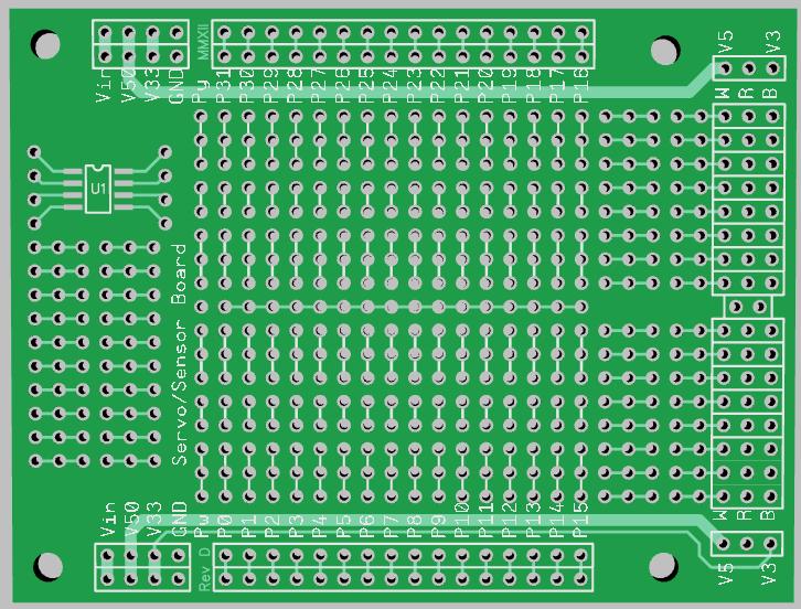
I'm working on a servo/sensor board (see attached) and would appreciate comments.
Yes, I know there are a couple traces I need to tie into the cooper pour (still looking for that).
I've placed a SOIC-8 breakout on this, but am starting to doubt this would be the handiest to have. Ideas?
Add thick 5v traces all around. Still needs copper pour to GND, cap pads?


OBC
I'm working on a servo/sensor board (see attached) and would appreciate comments.
Yes, I know there are a couple traces I need to tie into the cooper pour (still looking for that).
I've placed a SOIC-8 breakout on this, but am starting to doubt this would be the handiest to have. Ideas?
Add thick 5v traces all around. Still needs copper pour to GND, cap pads?


OBC


Comments
EDIT: I see you have a SOIC breakout there, I think it would be neat to make a shield that has several SMT packages on it as a breakout/protoboard. You'd have an SMT area and PTH area on the same board.
John Abshier
There are three jumpers: (two decide power options 3v or 5v for each row of 8, the center jumper allows connection from a single power jumper to cross all 16 connections. Removing the center jumper allows you to have a row of 3v items, and a row of 5v items.
The connections on the left are something I thought would be handy for linking the board to another PCB or breadboard.
OBC
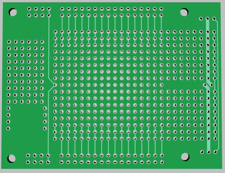
Traces...I couldn't agree more.. It's already on my todo list. I ran out of room on the top side and will move expanded traces to the bottom on the next revision. (sometime today).
BOC's.. I hadn't thought of that! Couldn't they side across one of the pin header positions between R & B when required, or would you consider them to be standard and work in a couple BOC points near the 5v/3v jumpers?
OBC
I'm "almost" happy with this design, got a couple more issues work out.
OBC
Those are voltage regulators, and they drop voltage, not current.
Looks like you have some room to fatten up the V33 supply lines also. Just for giggles.
Jim
Hey Sonic,
It would be great to use the "Reply with Quote" to be sure which reply you are addressing.
Just sayin'
Jim
I second John's Vin request.
You could make the jumper have three possible positions by placing a hole to the outside of each center hole. Right between the "V5" and "V3" silkscreens.
Yes, when it's finished I'll make the design Open Source.
OBC
I'm starting to run out of room for these thick traces, but something like this?
OBC
BTW, this is the template I started with... The .dip file is near the bottom of the page in the resources section.
Still playing with it, but I've got a lot of nice I/O traces on the bottom I don't want to sacrifice..
OBC
John Abshier
Yeah, my thinking too.. I'll keep fiddling with it until I find "elegant"
OBC
Here are some of my ideas (just keep in mind I have less circuit board designing experience than you). I like the SOIC idea; what about expanding on it? If you stagger the 0.1" holes (or just route the traces around the inner hole, you could a section to add multiple SOIC chips. This way one could add different combinations of SOIC chips, each having different amounts of pins.
I drew my guess at traces for the power lines (I drew only one side, but if you think it could work, you could do the same thing on both sides). I don't know if it's okay to run a line around the outside edge of not.
Now, that I've thought about this a bit, I think your idea (of having a jumper on the left side of the board too) is probably better.
It might be time to "flip" the entire design.
OBC