Shop OBEX P1 Docs P2 Docs Learn Events
Need feedback on this stepper driver board design — Parallax Forums

Need feedback on this stepper driver board design

pedwardpedward Posts: 1,642
edited 2012-01-11 01:36 in Propeller 1
I drew up a PCB for the L298 dual h-bridge driver, for testing and coding my software stepper driver code. I used the schematic from the datasheet and layed it out best as I could. I used the ExpressPCB software, it's free and their boards are quick and reasonably priced (please don't post about the half dozen Chinese board houses that can do a 10 part run for 89 cents each).

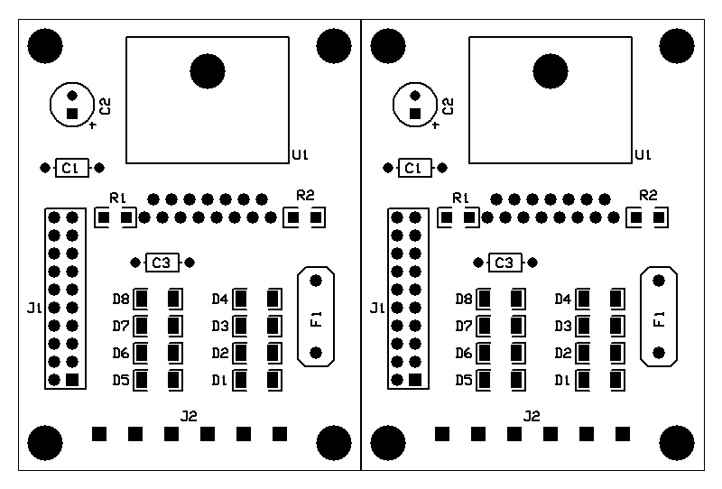
I designed it so it can either be piggybacked onto a board, or a header soldered to it and used with a breadboard, 2 drivers fit on a single 2.5x3.8 board.

I used SMT and other parts that I could order from Jameco, which was half the price of Digikey. The current sensors are 1/2w SMT chip resistors, I have a kit on hand so I designed for that. The current sense resistors are .1 ohms, so the range is always within what an MCP3202 can read without an external Vref needed. With a 3208 you could use an external precision voltage reference, such as an LM385-2.5 or such.

I just wanted to get feedback on the layout, I put a copper pour on the bottom layer for PowerM and on the top layer for Gnd, so the tab of the L298 can be soldered to the ground plane and the board used as a heatsink.

I have attached the various files for perusal.

EDIT: I added a PolyFuse to the circuit for current protection. These are self-resettable fuses that trip at a given current and reset once power is removed.

Schematic
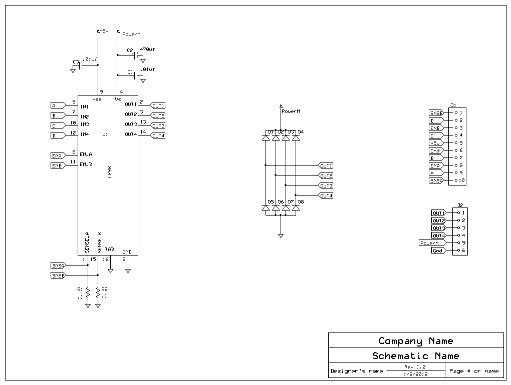
L298-001sch.png


PCB silkscreen layer
L298-001_silkscreen.png
1020 x 770 - 5K
800 x 542 - 7K

Comments

  • Phil Pilgrim (PhiPi)Phil Pilgrim (PhiPi) Posts: 23,514
    edited 2012-01-08 21:56
    I can't tell from the image file you posted, but I hope you have separate ground returns for Vss and PowerM ground and that they are joined only at the driver chip. Simply connecting both to the ground plane is not a good idea.

    -Phil
  • pedwardpedward Posts: 1,642
    edited 2012-01-09 01:16
    There are 2 grounds, the current sense grounds and the main ground. There is no separate ground for the logic portion. I used the poured ground plane to connect the grounds together instead of running individual traces. Could you give a reason why this is not a sound practice?

    EDIT: I went back and edited it to pour a ground plane on the top and bottom, and run dedicated traces for PowerM (for the motor). This seems consistent with several discussions I found on the net.
    L298-001_top_bottom.jpg
    1024 x 675 - 138K
  • Phil Pilgrim (PhiPi)Phil Pilgrim (PhiPi) Posts: 23,514
    edited 2012-01-09 09:29
    It's always helpful to think of a groundplane as a large resistor, rather than a sheet of copper, especially when large currents are involved. As such, the voltage at different points throughout the groundplane will vary. You have to ask yourself, "Where are the current pathways in my design? Where are the choke points? How can I steer those currents better so I don't create voltage differentials where I don't want them?" I call this the feng shui of PCB layout. You can steer current flow in several ways: moving parts and traces, creating separate traces for ground which rejoin the groundplane at a remote point, and putting cuts in the groundplane.

    In particular, in your design, examine the current pathway between R1 and the GND terminal.

    -Phil
  • pedwardpedward Posts: 1,642
    edited 2012-01-09 11:38
    Phil, here's another stab at it:
    L298-001_top_bottom.jpg
    1024 x 676 - 140K
  • Phil Pilgrim (PhiPi)Phil Pilgrim (PhiPi) Posts: 23,514
    edited 2012-01-09 13:38
    It's an improvement. But your logic ground is connected to the power return at three points: to the tab via the groundplane, at the GN pins on J1 on the bottom of the board (at least it looks that way), and to D5 via the groundplane. Also, I think the GND connections of R1 and R2 need to be much closer to the IC's ground pin:
    The sense resistor, not of a wire wound type, must be grounded near the negative pole of Vs that must be near the GND pin of the I.C.

    Basically, you want routing that looks like this:

    attachment.php?attachmentid=88382&d=1326145079

    In this schematic, the heaviest currents run along the red lines. You don't want these currents passing through the IC's ground pin, its tab, or J1's GN pin.

    -Phil
    467 x 486 - 4K
  • pedwardpedward Posts: 1,642
    edited 2012-01-09 14:06
    Thanks for the concise feedback, I can be dense at times, but I appreciate your patience.
  • Phil Pilgrim (PhiPi)Phil Pilgrim (PhiPi) Posts: 23,514
    edited 2012-01-09 15:38
    No problem. One more thing: be sure to connect the sense traces from J1 to R1 and R2 right at those resistors. You don't want to include the resistance of the traces from R1 and R2 to the IC in the current equation.

    -Phil
  • pedwardpedward Posts: 1,642
    edited 2012-01-09 16:12
    Phil,

    I reworked the layout a lot and came up with what you see below. Regarding the sense outputs, I sized the traces so they were .016 ohms each, so they are balanced. The layout just didn't lend well to putting the other sense very close.

    L298-001a_top_bottom.png
    514 x 680 - 16K
  • Phil Pilgrim (PhiPi)Phil Pilgrim (PhiPi) Posts: 23,514
    edited 2012-01-09 16:54
    That's looking better. The resistance of the sense line back to J1 does not matter, since it won't be carrying much current. It's just a voltage probe. So both can be the same small width. Don't forget to create a copper pour under the tab for heatsinking, and connect it to the ground pin.

    I would probably have connected M+ and GND to the center two pins of J2 and put R1and R2 where C3 is. Then you can run the A, B, C, and D lines around the back side of the IC hole pattern. That way the "T" shown in my schematic can be more properly positioned below the IC, and the sense resistors will be close to the ground pin. That does complicate the routing to C1 and C2, though -- at least where they're currently located.

    -Phil
  • Martin_HMartin_H Posts: 4,051
    edited 2012-01-09 17:07
    This was an interesting thread and I just learned something as an observer. I've done the exact same thing connecting power and logic grounds to a common ground, rather than keeping separate up to the L298. So far nothing bad has happened, but I will avoid this in the future.
  • pedwardpedward Posts: 1,642
    edited 2012-01-09 18:17
    I have poured a ground plane and connected the tab to it, I have the option of making all of the ground traces zero clearance so they touch the ground plane, or I can set a clearance and use specific connections at various points, what do you think?
    L298-001a_top_bottom_gp.png
    526 x 695 - 17K
  • Phil Pilgrim (PhiPi)Phil Pilgrim (PhiPi) Posts: 23,514
    edited 2012-01-09 19:03
    No. It's a step backwards, I'm afraid. Is there any way that you could follow my recommendations of posts 6, 8, and 10?

    -Phil
  • pedwardpedward Posts: 1,642
    edited 2012-01-09 20:02
    The difference between the last and previous was that I fixed the sense resistor connections and poured a ground plane. I have scaled the plane back to just be a heatsink, I'm not really certain what you didn't like about that pour, since it was essentially the same as before.

    Routing the power up the middle would require another complete redo, so I'm hesitant to reroute the power and fuse and diodes again.

    This is what I got, the tab is grounded to GND pin 9 and that is all.
    L298-001a_top_bottom_gp_small.png
  • Phil Pilgrim (PhiPi)Phil Pilgrim (PhiPi) Posts: 23,514
    edited 2012-01-09 20:23
    pedward wrote:
    I'm not really certain what you didn't like about that pour, since it was essentially the same as before.
    GN was connected to the groundplane, which included motor return currents, instead of only to the IC's ground pin.

    Although it's not the optimum layout, what you've got now will probably be okay. At least you've got the logic ground routed directly to the L298's ground pin and isolated from the motor return currents. Although I would prefer to see the GND connection of R1 and R2 closer to the IC's pin 8, what you've got will probably work. The only easy change I might recommend is to route GND directly to the copper pour -- not through R1 and R2 -- so you can provide heat relief on R1's and R2's pads. They might be a little hard to solder in the present configuration. (Heat relief vs. current capacity is one of those tradeoffs that always leads to compromise in a layout. It's unavoidable.)

    You haven't shown your solder mask layer. Just be sure that the copper under the IC pad is not covered with solder mask, in order to make a good thermal connection. You will definitely want to use thermal grease or some other heat-transfer medium.

    -Phil
  • pedwardpedward Posts: 1,642
    edited 2012-01-09 22:10
    GN was connected to the groundplane, which included motor return currents, instead of only to the IC's ground pin.

    The only easy change I might recommend is to route GND directly to the copper pour -- not through R1 and R2 -- so you can provide heat relief on R1's and R2's pads. They might be a little hard to solder in the present configuration. (Heat relief vs. current capacity is one of those tradeoffs that always leads to compromise in a layout. It's unavoidable.)

    You haven't shown your solder mask layer. Just be sure that the copper under the IC pad is not covered with solder mask, in order to make a good thermal connection. You will definitely want to use thermal grease or some other heat-transfer medium.

    -Phil

    I think I have understood what you said, one thing is that the Tab is GND and needs a large plane for heatsinking, so I was planning on soldering it to the ground plane directly. Do you see a problem with this? This is done on linear regulators and NPN transistors quite often, so I didn't think that would be a problem. The solder mask is tricky because they don't give you direct control, so I made 2 large SMT pads that will be exposed under the part, giving a tinned surface for soldering.

    Here is the latest rev, I re-did the layout to route power more like you suggested.

    EDIT: I fixed the close traces on the B and C outputs so there is the proper amount of minimum clearance.

    L298-001b_top_bottom_gp.png
    526 x 689 - 17K
  • Phil Pilgrim (PhiPi)Phil Pilgrim (PhiPi) Posts: 23,514
    edited 2012-01-09 23:10
    Much closer, but no, I'm afraid. Remember: the tab and IC ground are logic ground, not motor power return. The latter occurs through the current sense resistors. But you're going to solder the tab to the ground plane, which is the power return for the motors. I agree with soldering the tab to a copper pour -- that's great. But you need to pay attention to the current flows and isolate the motor currents from the logic currents.

    I don't mean to stress you, and any of your designs would probably work. But since you asked, I assumed a "teachable moment" was in order. :) If it's any comfort, I suspect that some of the issues with Parallax's MSR1 board could be traced to the same issues we're discussing here.

    -Phil
  • pedwardpedward Posts: 1,642
    edited 2012-01-09 23:18
    I will isolate the pour from motor ground and give it another try.
  • Peter JakackiPeter Jakacki Posts: 10,193
    edited 2012-01-10 01:02
    Can you get the L298 to lie horizontally on the PCB? The leads are staggered and formed for vertical insertion and it wouldn't be easy to get it to lie flat etc. There's another problem also with trying to solder a tab of this size to a large area of copper, you are going to need a very large soldering iron or some help from your local plumber. Then if you ever need to replace it................arrgghhh. (Yes, SMD parts are soldered this way, but they are much smaller)

    EDIT: I see that you can get them for horizontal mounting.
  • pedwardpedward Posts: 1,642
    edited 2012-01-10 07:58
    I revised the board a little, here's the final go-round:
    L298-001b_bottom.png
    L298-001b_top_bottom_gp.png
    514 x 693 - 13K
    522 x 684 - 17K
  • Phil Pilgrim (PhiPi)Phil Pilgrim (PhiPi) Posts: 23,514
    edited 2012-01-10 08:11
    I'm liking that a lot better! Do all the revisions make sense to you now?

    -Phil
  • pedwardpedward Posts: 1,642
    edited 2012-01-10 08:59
    Phil,

    Of course, the thing that I had to get reckoned was that you have to look at things backwards. The A and B Sense inputs should actually be treated as a dedicated circuit and not part of ground. I was working on the mental picture that Gnd on the chip was just Gnd, because it wasn't labeled "Logic ground", so it didn't click for me immediately.

    Of course, after doing this layout I have come to the conclusion that I should test it and put it on the shelf, then design a layout for DMOS drivers. :smile:

    I'm gonna fab up a batch of MiniBoards and build some drivers and work out my software, then worry about a "better" driver.

    I still want a discrete power driver design so the Prop can drive whatever it wants. I started thinking about DAC drive when I was hunting for chips and found an HDD spindle motor driver that does that (they call it voltage drive instead of source voltage control). The DAC drive reduces EMI because it's not chopping, so the driver generates a lot less noise. This approach could be used to drive any type of motor very cleanly.
  • pedwardpedward Posts: 1,642
    edited 2012-01-10 23:40
    Phil,

    I spent this evening redrawing the whole kit-n-kaboodle in DipTrace so I could make a PCB from gerbers, and to learn how to play with DipTrace. I have to say it's a nice product!

    I spent most of my time futzing with the placement of the diodes and such so that the autorouter wouldn't be stupid. I didn't spend any time manually routing the board, obviously I could improve the layout if I transferred it from ExpressPCB.

    Anyhow, here's a 3D render of the layout:
    l298-002_3d.png
    726 x 767 - 49K
  • Phil Pilgrim (PhiPi)Phil Pilgrim (PhiPi) Posts: 23,514
    edited 2012-01-10 23:51
    You already had a good layout. Why did you use an autorouter? (I hate those things. All they know about is connectivity and nothing about current flow issues.) BTW, you need heavy traces between R1/R2 and the IC, since they carry all of the motor current. Only the traces from R1/R2 to J1 can be narrow, since they do not carry significant current.

    -Phil
  • pedwardpedward Posts: 1,642
    edited 2012-01-11 01:36
    I was just tinkering with Diptrace, my motivation was to try and make some gerbers I could etch at home. The layout is more for education and learning the program, rather than full design rule checking.

    Here's the final tweaked render:
    l298-002_3d.png
    736 x 787 - 49K
Sign In or Register to comment.