

Memsic 2125 Accelerometer on 2 Wires
 Phil Pilgrim (PhiPi)
Posts: 23,514
Phil Pilgrim (PhiPi)
Posts: 23,514
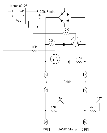
I have an app in mind that requires a short cable run to a Memsic 2125 Dual-axis Accelerometer. It's desirable in this app to use as few conductors as possible to connect to the remote sensor. So I came up with a way to interface the Memsic to a BASIC Stamp over a two-conductor cable that provides power and receives the Memsic's PWM output from both axes. Here's the schematic:
 'Just noticed an error. The X and Y labels for the cable and Stamp are reversed.
The BASIC Stamp's outputs provide power during a charge phase, in which one pin is raised while the other is brought low. This keeps the Memsic's supply capacitor charged long enough for the readout phase. My testing was done with a 1000µF cap, but it looks like a 220µF device will work, too, without excessive discharging during readout. In the readout phase, the pin that was high is changed to an input. This allows the transistor whose collector is connected to the positive line via a diode and resistor to pull the line down against the pullups on the BASIC Stamp's end of the cable. In this way, the BASIC Stamp can read the period and duty cycle to determine the degree of acceleration/tilt on the associated axis. To read the other axis, the process is repeated, but with the roles of the two conductors reversed.
You might wonder why the diodes are necessary in series with the transistors. It's because bipolar transistors have a secondary conduction mode in which the emitter acts like a collector and vice-versa. Without the diodes, the non-selected transistor has enough drive in this mode to affect the output waveform. The diodes prevent this from happening.
Here's the PBASIC program I used for testing:
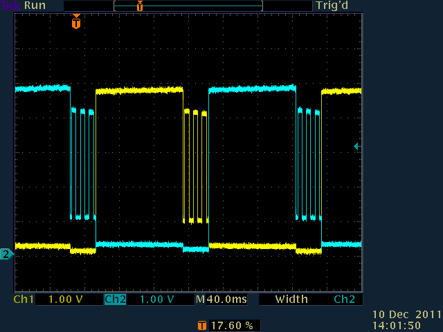
And here's what the two conductors connecting the Stamp to the sensor circuit look like on my scope:

The readout phase lasts just long enough to catch one high pulse and one low one, plus a little PBASIC overhead. Then the charge phase for the other axis begins.
The pullups are a bit wimpy to work over a long cable without picking up noise. If they're decreased, the value of the collector resistors also has to be decreased to keep the low pulse tips below the BASIC Stamp's logic threshold. But my app needs but a short cable, so the values I've selected should work out okay.
-Phil
The BASIC Stamp's outputs provide power during a charge phase, in which one pin is raised while the other is brought low. This keeps the Memsic's supply capacitor charged long enough for the readout phase. My testing was done with a 1000µF cap, but it looks like a 220µF device will work, too, without excessive discharging during readout. In the readout phase, the pin that was high is changed to an input. This allows the transistor whose collector is connected to the positive line via a diode and resistor to pull the line down against the pullups on the BASIC Stamp's end of the cable. In this way, the BASIC Stamp can read the period and duty cycle to determine the degree of acceleration/tilt on the associated axis. To read the other axis, the process is repeated, but with the roles of the two conductors reversed.
You might wonder why the diodes are necessary in series with the transistors. It's because bipolar transistors have a secondary conduction mode in which the emitter acts like a collector and vice-versa. Without the diodes, the non-selected transistor has enough drive in this mode to affect the output waveform. The diodes prevent this from happening.
Here's the PBASIC program I used for testing:
' {$STAMP BS2}
' {$PBASIC 2.5}

xpin    PIN 0
ypin    PIN 1

xpos    VAR Word
xneg    VAR Word
ypos    VAR Word
yneg    VAR Word

DO

  LOW ypin
  HIGH xpin
  PAUSE 100
  INPUT xpin
  PULSIN xpin, 1, xpos
  PULSIN xpin, 0, xneg
  DEBUG SDEC (xpos - ((xpos + xneg) >> 1)), " "

  LOW xpin
  HIGH ypin
  PAUSE 100
  INPUT ypin
  PULSIN ypin, 1, ypos
  PULSIN ypin, 0, yneg
  DEBUG SDEC (ypos - ((ypos + yneg) >> 1)), 13

LOOP
And here's what the two conductors connecting the Stamp to the sensor circuit look like on my scope:
The readout phase lasts just long enough to catch one high pulse and one low one, plus a little PBASIC overhead. Then the charge phase for the other axis begins.
The pullups are a bit wimpy to work over a long cable without picking up noise. If they're decreased, the value of the collector resistors also has to be decreased to keep the low pulse tips below the BASIC Stamp's logic threshold. But my app needs but a short cable, so the values I've selected should work out okay.
-Phil
640 x 480 - 15K
453 x 560 - 5K
Comments
What a great circuit!