

I'd like someone to look at my schematic and PCB design for comments
 Don M
Posts: 1,654
Don M
Posts: 1,654
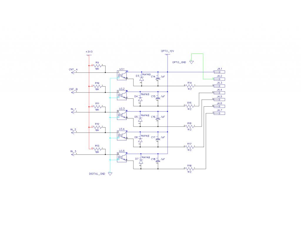
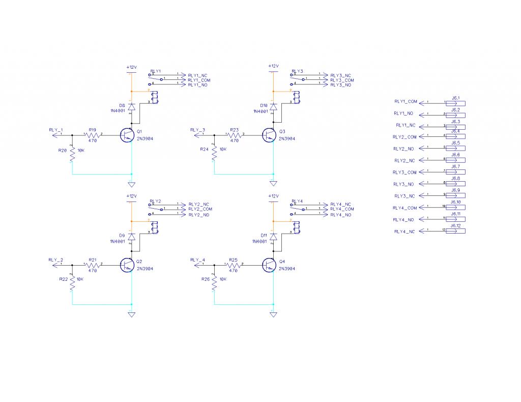
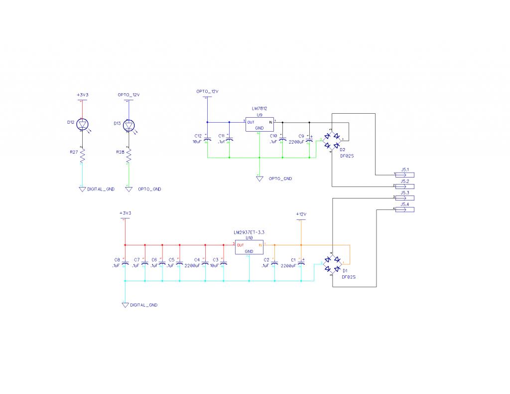
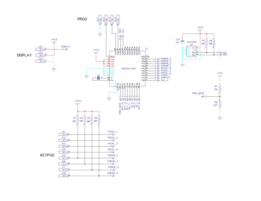
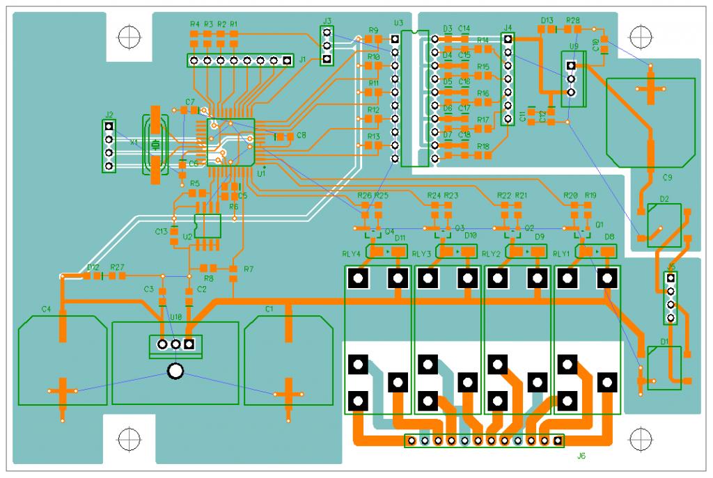
Before I fire it off to the PCB house I'd like any constructive comments on the design and layout. This design is replacing an existing board and the components and connectors are in strategic locations and can't be moved much. I drew it in Diptrace but am presenting it here in graphic format for all to be able to see.
Thanks in advance.
Don


Thanks in advance.
Don
1024 x 790 - 35K
1024 x 790 - 50K
1024 x 687 - 110K

1024 x 790 - 46K

1024 x 790 - 40K
Comments
Those acute angles where tracks are joined are a bad idea, they act as acid traps when etching and look ugly. They should join at right angles.
The routing could be tidied up a lot.
You seem to have some nets that haven't been routed. Have you generated a net completion report?
I'll look at changing the angled intersections into right angles. As simple as this board may look it was rather difficult to access so many prop pins at least for me anyway.
Thanks for the suggestions.
PCB Design Tutorial