

First PCB - Please Check
 mhamen3
Posts: 69
mhamen3
Posts: 69
Hi guys,
I've designed a board for a project I've been working on http://lynxmotion.net/viewtopic.php?f=8&t=7256. It has an Xbee module in the upper left, 3 I/O Headers (2 for servos run at 7.4V with their own battery terminal and 1 for 4 hall effect sensors to read shaft rpm which can be jumpered to 5v), in the upper middle there are 2 pin outs for TB6612FNG motors drivers. There will be two driver boards stacked on each pin out. I'll be driving 4 motors but will be running the boards in parallel. There's the power supply on the right and the eeprom and prop plug header on the left of the prop.
Please review this; any criticism is welcome. It is still a work in progress and is still kind of crude. This is my first time designing a board and I know there are some things that I must be overlooking.
Thanks,
Marc
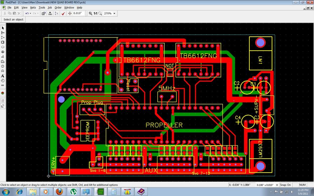

1024 x 640 - 123K
Comments
Lawson
The Servo + seems to be connected to ground, at least to the EEPROM... have you checked that the schematic and the board are consistent ? (that they match ?)
And a LED to indicate that power is applied to the board is a life-saver more than once
Edit: Have you built a prototype to check that everything works well ?... before committing to some PCB ?
Schematic? Hmmm... I didn't make one. Did I mention this was my first time? Ha
I will be sure to add the decoupling capicitors to the prop, xbee, and drivers, and to finish routing the NOT and reset. Also, to change the ground connection for the eeprom: I would have totally missed that.
I would like to add a power LED but I'm not quite sure how to do it. Simple I'm sure but its been a few years since I've taken electronics courses (I'm an ME) and anything outside of blackbox operation is beyond me. For mounting holes I have a lone one on the left and figured I could just use the holes from the regs on the right.
As for the QFD prop, I thought about it but I already have a few of the DIP so I'm just going to stick with that.
I'll revise tonight.
Thanks again guys,
Marc
Although I have had no problems with it, it is generally recommended that there are no 90 degree track bends, use a short 45 degree bit. This is to prevent the etchant getting in and undercutting at the corner, I think.
And I agree with Leon: start with a schematic.
Decoupling caps are a must: one for each Vdd - Vss pair. You can hide them under the Propeller DIP, if you plan on using a socket. Once, I assembled a panel of prop boards and tested each board before adding decoupling caps - just by testing, I ended up burning out the PLL's on about half of 'em.
How difficult is it to make your own board (I have a small cnc mill). I have found a site ( www.pad2pad.com) that has quoted my board for just under $70 shipped for 3 boards. However, if I wanted to add the ground plane, BOOM, it shoots up to over $300.
http://dorkbotpdx.org/wiki/pcb_order
Presumably that made it a four-layer board, which isn't necessary. It's very expensive, though, I can get them made much cheaper than that.
Join the Homebrew-PCB Yahoo group if you want to make your own PCBs. I use photo-etch, it's very easy.
All of my designs with ground plane have been two layer. For boards with a simple layout, like yours, you can often fit 95% of the non-ground traces on one layer. The second layer is then just ground plane, and short jumpers where two wires cross. I've got several boards designed like this that live near a Pockels cell. (switches 4Kv in a 1-2ns, unshielded it induces ~10Vp-p in a 3 inch loop of wire at ~4 feet.) Whatever noise that does couple into the power rails is unmeasurable. (<1mVrms with our oscilloscope)
Lawson
That's true, I got it wrong. I wondered why there was such a leap up to more than the two easy layers. As I never get the chance to do commercial boards I had not considered internal layers.
What I meant was copper pour, which can amount to 90% of the layer.