NAND logic circuit questions
Hello everyone,
I am making an event timer that will use an IR LED and photo transistor pair (Radio Shack 276-0142) to start the timing, and an identical pair to stop the timing.
I've got that part working. Idle is .95 volts, start pulse goes to 4.88 volts and immediately back to .95 volts. An instant later, the stop pulse goes from .95 volts to 4.88 volts, and immediately back to .95 volts.
I am using a BS2p40 PULSIN command for the timing. The timing "window" is long enough for what I am doing. So with the logic circuit, I have to make the start pulse make the stamp Input pin go High and latch and start the PULSIN counter, and then when the stop pulse hits, the stamp pin needs to go Low to stop the PULSIN counter.
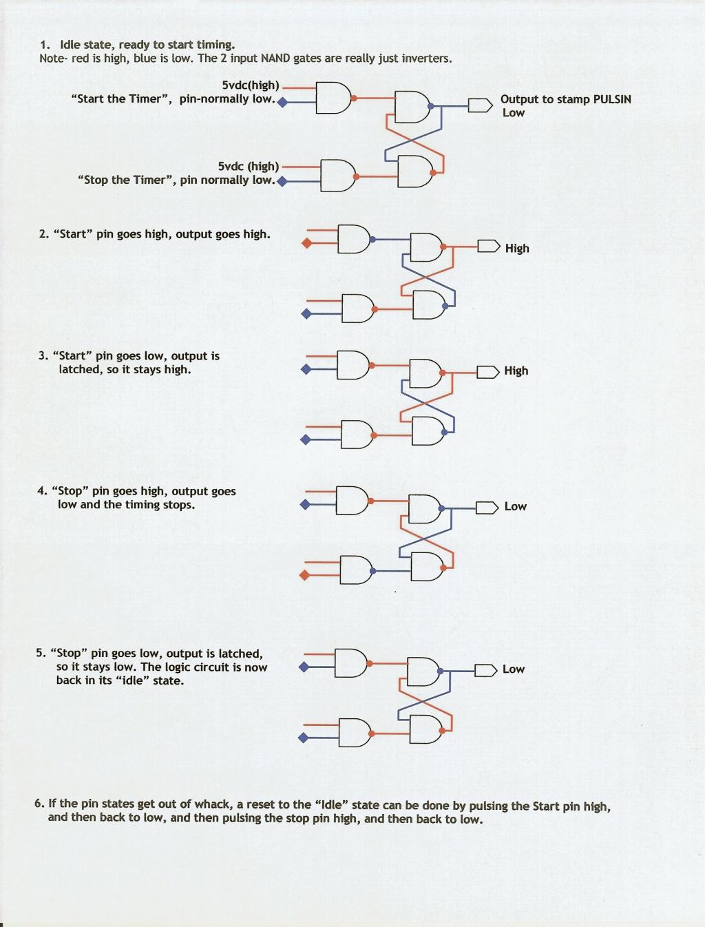
I have a MC14011 quad NAND gate and have drawn out what I think the sequence of events will be.
I used http://www.play-hookey.com/digital/rs_nand_latch.html
to try out the logic states, and they seem to work.
So the first part of the question is: does it look like the logic will work, including the manual reset feature?
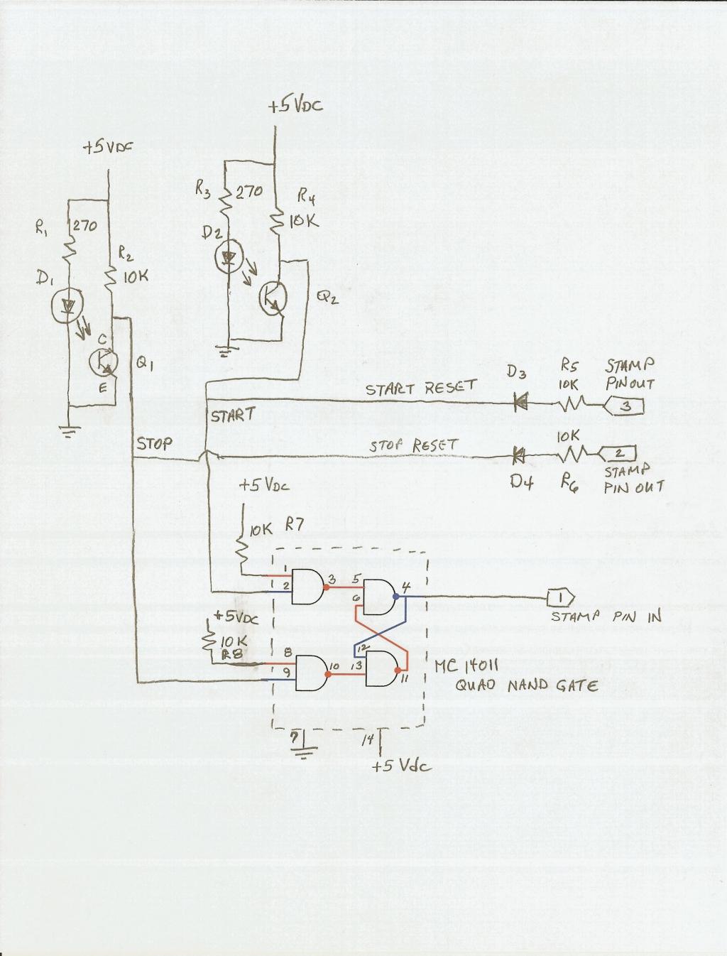
The second part is the circuit itself. I've got the photo transistor part working. As I said, normal idle state is low, and blocking the IR path makes the output go high.
One of my main concerns about the circuit is the two stamp pins I have for a reset function. Do they look OK? Are the diodes necessary? Do I need additional diodes? Will the reset pulses from them actually be able to reset the NAND gates to the desired "Idle" state?
I am attaching a jpg of the logic, and a jpg of the circuit.
Thanks for your help,
Lloyd


Comments
I added a 0.01 cap between MC14011-14 and gnd. Added 470 ohm resistors between the photo transistor collectors and Mc14011-2 and 9. Don't really know if either of those changes were necessary, but they seemed to make sense.
I didn't hook up the 2 stamp pins for the reset feature and it kinda looks like i might not need it.
Lloyd
Wow, that certainly is a lot easier than what I am doing. Unfortunately I need almost all of the 0.8 micro sec resolution of the 2p to get the correct timing. Total event duration is about 500 microsec, but the differences from event to event are itty bitty!.
I've put another post for the follow-on problem I am having.
Thanks,
Lloyd