

EEPROM hook up and usage issues
 Stampmyster
Posts: 27
Stampmyster
Posts: 27
This is my first attempt to use EEPROM integrated circuits. Im using (2) 24LC128s and a BS2. I find the whole business confusing especially trying to make sense of commands like SHIFTIN, MSBPRE, MSBFIRST
etc. However, using modified example code, hook-up examples, perseverance and a lot of trial and error I did manage to make something work.
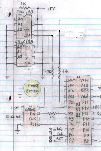
The main issue Im concerned about is the wiring. The first one is hooked up as A0 and the second as A1. Trouble is, I have to declare in the code that A1 is A2? (See wiring diagram and code.) If I hook up the second EEPROM as A2 (As I think it should be.) it doesnt work at all?
I would bet a cookie, Im simply not grasping the full concept. Any suggestion or solutions would be greatly appreciated!
383 x 574 - 46K

Comments
In looking at your circuit, you have a couple of errors. From your "top" EEprom you have the SCL (Signal clock line) going to the SDA (signal Data line). This will confuse the EEproms. So what you will need to do is run the SCL from the TOP EEprom to the SCL line on the bottom EEprom. Then do the same for the SDA lines. One of the other things I see is that the two 4.7K resistors are in the incorrect place. What you'll want to do is run one resistor from your SDA line to +5v, and the other resistor from the SCL to +5v. Right now your have them in series with both lines. This should help on th hardware side.
Anyway, the original problem still exist.
Any suggestion or solutions would still be greatly appreciated!
Well one thing to remember about this I2c stuff is you have to think of it like cities. The first EEprom you have wired up (actually hard wired up, the one on the bottom) is Address 0. You have A0, A1, A2 all wired to ground, so that is a binary 0. When you tell the Stamp to write/or read to the chip wired as address 0, this is the chip that is going to be selected. Think of this as the City, now within that chip are more addresses of many places to read/write from. I guess you can think of them as the mailboxes for people who live in that city. These are the addresses of where to store or read data to/from, but they are all "within" these chips.
The next chip up the line (the top one, or the next city along the highway) you have hard wired as address: 1 This is because A0 is tied to V+ and A1, A2 are tied to ground. This represents a binary 1. Now for example (on the top chip) if you had A0 wired to ground, A1 wired to +5, and A2 to ground, that would be at address 2 (or binary 2) for this chip.
In quickly looking at your code I noticed where you have the "enter 0 or 2 for A0 or A2" input, your are setting your variable Address = hex A0 or hex A2. Try changing A2 to A1 and see if that helps, since Address 1 is the value set for your top EEprom. According to your schematic, you currently do not have any chips (or EEproms) wired up as Address "2". You only have Address 0 and Address 1.
Hope this helps a little more.
http://forums.parallax.com/showthread.php?126798-NEW-EEPROM-expansion-%28bank-switch-adapter%29
It can also act as a handy carrier board for a couple EEPROM chips and instead of the jumper you can hard wire it for A0 and A1 by just keeping the same pins shorted. It also has pads to add optional pull-up resistors on the SDA and SCL lines.
Robert
Yep, the first chip is wired up as $A0 (%1010 0000) and appears to be working normally.The second chip appears to be wired up as $A1 (%1010 0001), and that is the issue! The software still sees it as $A2 (%1010 0010)??
I tried changing the code to $A1 and it simply doesnt work. I even tried different wiring schemes and new chips (24LC256) with the same result?? $A1 seems to address nothing??
Im starting to wonder, if there is 32,000 bytes on each chip, and the code only allows addressing to 16,000 bytes, perhaps $A1 is actually inside what we are calling the $A0 chip? Thus, the second chip starts at $A2??
But, how do I know or sure? And how would I do it? :blank:
I keep staring at the data sheet, and mostly what I get most out of it is that Im in totally unfamiliar territory. However this quote from 2.1 it does talk about how these logic pins can be controlled by a microcontroller and internal circuitry to change address state:
2.1 A0, A1, A2 Chip Address Inputs
The A0, A1 and A2 inputs are used by the 24XX256 for
multiple device operations. The levels on these inputs
are compared with the corresponding bits in the slave
address. The chip is selected if the compare is true.
For the MSOP package only, pins A0 and A1 are not
connected.
Up to eight devices (two for the MSOP package) may
be connected to the same bus by using different Chip
Select bit combinations. If these pins are left
unconnected, the inputs will be pulled down internally
to VSS. If they are tied to VCC or driven high, the internal
pull-down circuitry is disabled.
In most applications, the chip address inputs A0, A1
and A2 are hard-wired to logic 0 or logic 1. For
applications in which these pins are controlled by a
microcontroller or other programmable device, the chip
address pins must be driven to logic 0 or logic 1
before normal device operation can proceed[/SIZE]
So, to make a long story short, Im not out of the woods yet, and continued advise or solutions are truly welcome!
However, I’m not sure what changing to a 10K resistor would do for me?
Unfortunately, I don’t have the luxury to physically flip a switch. Simply, I will be recording time, temperature and a few other parameters once every hour for months at a time.
However, I believe, a switch could be rigged to swap chips by physically changing the wiring scheme with software, perhaps using transistors or relays, but I would rather take advantage of the built-in feature(s) that allows this to be done with code, without any additional hardware.
Still, creative solution, and surely would work in a pinch!
$A2 and $A3 address the 2nd chip (#1) and $A4 and $A5 address the 3rd chip (#2).
Look carefully at pages 8-11 of the documentation.
I had a sneaky suspicion that was what is going on!
OK, back to the books...
It appears you are saying the LSB in what they call the Control Byte determines the A0 A1access? This data is sent in the first two write cycles (required for either read or write operations)?
Alright, I think I have a grasp of what is going on now.
This:?
Control_Byte_Write: ' I2C Control Write Byte Sequence
i2cWork = Address
i2cWork.BIT0 = 0 ' Sets Unit To Write
SHIFTOUT SDA, SCL, MSBFIRST, [i2cWork\8] ' Send Byte To Device
SHIFTIN SDA, SCL, MSBPRE, [i2cAck\1] ' Get Acknowledge Bit
RETURN
I want to totally understand what is going on here and not just blindly fix it. I have to admit, I need to get out the command reference book and study the SHIFTOUT and SHIFTIN commands better.
At least I may have a clue to order and purpose and what to look for.
Awesome! Thank you all!
-Be Back
First thing I recognized was the “i2cWork.BIT0=0”
Well, if one can simply modify the first bit (R/W) this way, then why not the Second one (LSB) Simply add the statement “i2cwork.BIT1=1” in the read write subroutines?
Now, I think, it is a matter of managing the human-interface so the user can select which Chip and which Bank ($A0 or $A1) to access!
Control_Byte_Write: ' I2C Control Write Byte Sequence
i2cWork = Address
i2cWork.BIT0 = 0 :i2cwork.BIT1=1 or 0 ' Sets Which Device and where to Write
SHIFTOUT SDA, SCL, MSBFIRST, [i2cWork\8] ' Send Byte To Device
SHIFTIN SDA, SCL, MSBPRE, [i2cAck\1] ' Get Acknowledge Bit
RETURN
Control_Byte_Read: ' I2C Control Read Byte Sequence
i2cWork = Address
i2cWork.BIT0 = 1 :i2cwork.BIT1=1 or 0 ' Sets Which Device and where to Read
SHIFTOUT SDA, SCL, MSBFIRST, [i2cWork\8] ' Send Byte To Device
SHIFTIN SDA, SCL, MSBPRE, [i2cAck\1] ' Get Acknowledge Bit
RETURN
Nice!
Thank you
I’ll take a peek at the Nuts and Volt article now…. I also want to give the BSp a look see and try, as the I2c IN/OUT appears to be mighty powerful command….
I have attached a wiring diagram of (2) two 24LC256 EEPROMs (Item code 602-00032) with a total of 64,000 bytes of EEPROM !
I have also provided example code that allow one to access each location by it’s decimal address. For instance one can read or write from location 00000 all they way up to 63999. Each location can store one byte of info (0 - 254).
This program is poorly written as far as human interface is concerned, however it works well, and is intended to be used as an example and template for writing one’s own program. One can make it as fancy-dancy, or as simple as they like.
I really didn’t write anything, it is modified from example code for the 16KB ram chip located in the “Download and Documentation” section offered with item description in the online Parallax store.
Hopefully it will serve as a tool for others, to help understand the I2c protocol and learn to use multiple EEPROMs.
My application:
I intend to use EEPROM to record temperature, time, date, and other data on a project of mine. This data will automatically be stored every hour, 16 hours a day. (10 bytes of data ever hour) This will allows data to be stored for 6400 hours, or 16 hours a day for 400 days. That’s over a year!
I now realize, that I don’t need to record the time and date, as I know every 10 bytes of data equates to a “new” hour, and knowing the starting time and date, I can calculate the address with a calendar!
Example: If I started recording data on January 1st, at 12:00 AM, and wanted to access the data stored on July 4th at 2PM , the address would be 29740 to 29750 (Assuming 10 bytes of data is recorded at the top of each and every hour)
This, will allow more EEPROM for storing data and less code that tends to eat away at the program and variable space on the BS2.
I would be curious to hear about other schemes in this regard.
Again,
Thanks!