

My first PCB
 Microcontrolled
Posts: 2,461
Microcontrolled
Posts: 2,461
Now that N&V has finally paid though, I can do something I've always wanted to do: Get a PCB made!
I've had this design in my toolbox for a while now, and have been waiting until I could afford to get a run of them made. It's a module for the Propeller Chip (what do I make WITHOUT a Propeller chip anyway??) that is compact, uses all through hole parts, and is designed to work off of a battery. Since the point of it was to be as small as possible, it doesn't include any power converters or regulators. The headers are set up to be compatible with Gadget Gangster protoboard modules, although due to the limited width, only if all the connections are on one side. I've attached images. I'll be sending these boards off soon. If anyone has any advice beforehand let me know.
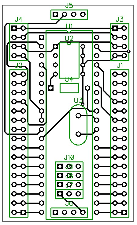
I've had this design in my toolbox for a while now, and have been waiting until I could afford to get a run of them made. It's a module for the Propeller Chip (what do I make WITHOUT a Propeller chip anyway??) that is compact, uses all through hole parts, and is designed to work off of a battery. Since the point of it was to be as small as possible, it doesn't include any power converters or regulators. The headers are set up to be compatible with Gadget Gangster protoboard modules, although due to the limited width, only if all the connections are on one side. I've attached images. I'll be sending these boards off soon. If anyone has any advice beforehand let me know.

448 x 733 - 120K
Comments
It would be great if you could post the schematic for the PCB, its hard to tell if the board layout is correct without the schematic.
I don't see any filter caps on the PCB, you need them.
Is the PCB a single sided board?,
From what I can see in the picture, I think it is.
Is the the stuff shown in green silk screen marking.
The marking for J7, J8, J9 is located on top of pads.
Is the picture showing the solder side or component side of the PCB.
The parts labeled U3 and U4 don't appear to be Integrated Circuits so they probably should not be labeled "U"
Regards,
zappman
Is there another side?
I don't see a way to program it with a Prop Plug. I also don't see the grounds connected to anything.
Plus what zappman said.
Think of the size it could be with a surface mount Prop. They are not that hard to solder.
What happened to your video Prop idea? Is this going to have any way of outputting video? I suppose you could have a small secondary board that plugs into some headers.
Have you decided who you'll have make it? I think SparkFun's BatchPCB is amoung the cheapest for small orders but I think they are kind of slow.
Duane
I forgot about the video idea, and SMD props would really cut down board space. Maybe this calls for a redesign.
I'm using BatchPCB to get them made. This one passes the test and according to them it only cost $8.75 to make! I think I'll resubmit it after I optimize the design, though.
It looks like U2 (I assume the EEPROM) has been mirrorred. The right four pins are all joined where normally the left four pins are joined (and connected to ground).
Duane
And the advantage to using all surface mount parts is that it's decreased the board space, and the price, by half!
Images attached of top AND bottom. I have this uploaded and checked by BatchPCB.
I'm pretty sure it's recommended to have 0.1uF decoupling caps close to each Vdd pin.
I'd also suggest pull up resistors on both the I2C data on I2C clock lines. (I think the data line is required.)
Is J5 for an upside-down Prop Plug? (I have one of those on one of my homemade boards but it wasn't purposefully upside-down.)
I looks like R1 - R3 would benefit from being turned 180 degrees.
What are J2 - J4 for?
I personally would rather have different pins connected to J1 since P30 and P31 are used in J2. I'd actually like to have a lot more pins available.
Duane
Before I order these, I'm going to have to find an effective way to solder SMD parts.
I like this board more than the last one. I still don't see any decoupling caps.
I'm no expert. I've played with Eagle a bit but I've never had one of my boards made. (I have etched a couple at home.) Someone with more experence will probably have more useful suggestions. I do see several 90 degree turns in your traces on the back side of the board. Apparently these can cause problems with high speed communication (and many people seem to think they look bad).
One of the crystal traces moves to the bottom of the board without any apparent need. It could take a relatively direct route to the crystal.
I'd imagine J1 and J6 are spaced at some multiple of 0.1". I hope so because it would make it easier to use with perf board or possibly a breadboard.
At least add the decoupling caps before having the board made.
If not, there should be more fat commons.
Yes?
A good location to place a capacitor for the top Vdd pin is right where the characters "U1" are located. I've also read each Vdd should have a decoupling cap so three other capacitors should placed so one is close the each of the other Vdd pins.
Again, I'm no expert. I'm just relaying advice I've seen other forum members (who are experts) give concerning other Propeller custom circuit boards.
I'd use the tiny 0603 size 0.1uF capacitors to save space.
OBC
I assume J5 is for a Prop Plug? If so, the Prop Plug would need to be plugged in upside-down.
The trace to the negative side of C3 sure takes the scenic route.
As Pliers mentioned earlier, Often ground traces are made wider than the rest of the traces. On the Propeller Proto Board Just about every area of the board not being used some other way has the ground extended to it. I don't know how much you need to worry about the ground plane or fat ground traces on your board.
I really do think you should fix the Prop Plug connection.
What program are you using? I'd assume it's either Eagle or DipTrace?
I think you're getting close to having a useful board.
@Duane Degn: I've always assumed that you inserted the Prop Plug sticker down, and that the other way was wrong! That's how the PE kit does it, anyway.
I'll see if I can get the copper pour working or not, then I'll post that version for verification then off it goes!
You're right (I just looked), it is upside down in the PEK instructions. I asure you everwhere else it's used rightside-up.
Edit: I haven't looked at the latest one yet.
I promise the sticker should be rightside-up.
BTW, I am using DipTrace
Bummer!
How is it flipped? If it's upside down, I suppose you could just remember to plug the PropPlug in upside down with this rev of the board..
Before submitting your design, you need to do a couple things:
1. Remove any groundplane segments that are not connected to anything. (The software should have done this for you.)
2. Check to make sure that you have connectivity among all your ground pads. It's not clear from your images that you do. (The software should warn you or produce an error if this is not the case.)
-Phil
See Verification/Net Connectivity Check.
These have everything done to them requested since my previous post.