

My first Diptrace drawn board....
 Don M
Posts: 1,654
Don M
Posts: 1,654
Took a while to get it all together but I think it turned out ok. Sent off for manufacture today to Pentalogix.

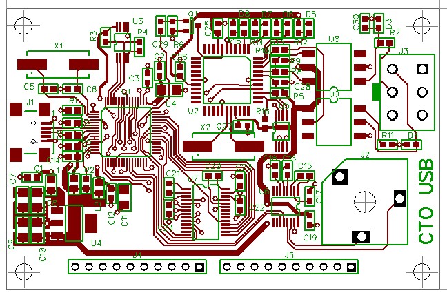
648 x 431 - 137K
Comments
Nice board lay-out Don M.
'
Could you snap a pic of it when you get it back from the board house and post-it?
'
I would really like to see it!
My boards are due in tomorrow. Parts came in today. Boy those 0603 resistors and caps are sure tiny!
Here's a couple photos of the board. They turned out very nice. This was my first time using the "toaster oven" reflow process. I am happy with that as well. In the beginning I thought I would hand apply the solder paste. Glad I changed my mind and had a stencil made. Worked pretty well but had a small learning curve to get the paste on right.
Regards,
Stanislav Ruev
DipTrace Team