

a question of linear voltage regulator circuits...Answered & Closed
 davejames
Posts: 4,047
davejames
Posts: 4,047
Hi All - Merry Christmas!
I have subject of discussion for the analog/linear forum members concerning voltage regulator circuits. And, please, no responses about the use of switch-mode supplies - thanks.
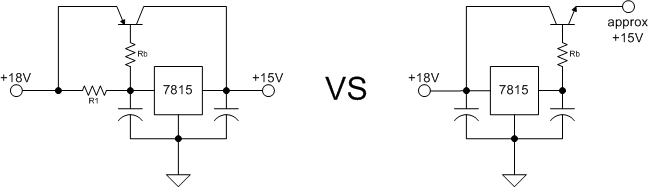
Ive been pondering two approaches for increasing the available current beyond that of what a regulator can provide (see attached diagram).
The circuit on the right is my simplistic approach (at least in my mind!). The idea is that the NPN transistor would be used as an emitter-follower with the emitter voltage being a tad less than the regulator voltage (Vreg - Vbe). All of the current would flow through the transistor. A variable output regulator could be used for compensating Vbe loss.
The circuit on the left is the typical result of InterWeb searches; a bit more complex as its a shared-current approach. The idea being that the regulator would handle the current up to 1A. Beyond that, the regulator current through R1 would begin to develop enough voltage to bias on the PNP transistor, which in turn would allow current to flow and join with the regulator current. Its a cool solution.
So, if you would, roll these two approaches around the grey-matter and give me your thoughts?
Much Thanks,
DJ
I have subject of discussion for the analog/linear forum members concerning voltage regulator circuits. And, please, no responses about the use of switch-mode supplies - thanks.
Ive been pondering two approaches for increasing the available current beyond that of what a regulator can provide (see attached diagram).
The circuit on the right is my simplistic approach (at least in my mind!). The idea is that the NPN transistor would be used as an emitter-follower with the emitter voltage being a tad less than the regulator voltage (Vreg - Vbe). All of the current would flow through the transistor. A variable output regulator could be used for compensating Vbe loss.
The circuit on the left is the typical result of InterWeb searches; a bit more complex as its a shared-current approach. The idea being that the regulator would handle the current up to 1A. Beyond that, the regulator current through R1 would begin to develop enough voltage to bias on the PNP transistor, which in turn would allow current to flow and join with the regulator current. Its a cool solution.
So, if you would, roll these two approaches around the grey-matter and give me your thoughts?
Much Thanks,
DJ
653 x 187 - 10K
Comments
DJ
Things like that.
Regards,
DJ
Thanks - that was the missing piece.
DJ
I disagree, Leon--The circuit on the left won't effectively prevent the burnout of the pass transistor in the event of a short circuit at the output. The circuit does on the left does have the optional resistor in series with the base, which could provide current limiting based on the transistor gain, but that is a very weak protection, and transistor gain varies widely from unit to unit and also with temperature. The transistor is in danger to burn out with a short circuit in either circuit. The data sheet also shows a standard circuit (attached) with one more transistor added to actively shunt the base current, which does in fact provide strong current limiting at the expense of a little higher input voltage.
The main advantage of the circuit PNP pass circuits that they really do regulate at 15 Volts and allows a larger current than can be provided by the regulator alone. The circuit with the emitter follower does allow more current but subtracts about 0.6 V for the base-emitter drop. That may be okay for some purposes. In either circuit the external pass transistor has to be chosen to handle the necessary power and current.
In fact, this is the sort of interaction/discussion for which I was hoping.
I see how Q2 turns on, but help me out here, I don't see Q2's return current path. Where does the current go so's to act like a shunt?
Thanks much,
DJ
P.S. I'm going to "un-close" the thread...
What is the current path? The Q2 emitter-collector current flows from the power supply thru the 78xx regulator and back to the power supply.
DJ
But now I see the MJ15003 in available and offers double the output specified by the 2N3055 or the compliment which is the MJ14004. Rated at 20 amps tops, that should be enough current for just about anything plugged into the average wall plug.
Here is a late addition to my 2 cents -- DIY 2 transistor regulators.
http://www.4qdtec.com/theory/2TrRegs.html
@Loopy - yeah, I'm beginning to agree. I'm always looking for the simplest design, but doing that sometime misses potential failure modes.
Overall, this has been a great exercise!
Thanks much and Merry Christmas,
DJ