

A protoboard for the Gadget Gangster Propeller Platform
 schill
Posts: 741
schill
Posts: 741
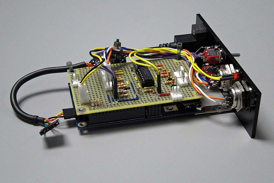
This is a basic protoboard that I designed for use with the Gadget Gangster Propeller Platform (www.gadgetgangster.com). Like most protoboards, its designed to provide a convenient generic workspace for laying out circuits.
Im not planning to mass produce or sell these boards and I thought people might be interested in the design. The expresspcb pcb file is attached if anyone wants to make one as is.
The board is sized to match the larger platform boards and, consequently, the 3 for $51 size from expresspcb (www.expresspcb.com). Unfortunately this board does not qualify for that price because it has too many holes.
Some basic features:
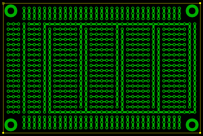
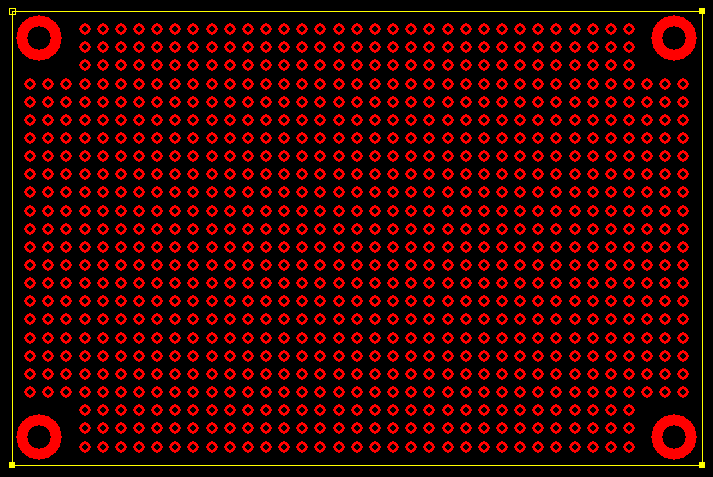
1) Most of the board is designed using a pretty standard breadboard-type distribution of pads and traces. The busses are available throughout the board. At one end of the board are sets of pads originally intended for creating offboard connections but they can be used for any purpose (including mounting chips). For example, it is very easy to connect breakout boards and adapters with single rows of pins to these pads. Unused platform pin pads on the long sides of the boards can also be used for this purpose. There is an extra set of connected pads running across the width of the board at this end which can be connected to either of the busses or used for distribution of other signals.
2) There are no pads specifically assigned to any of the pins from the Propeller Platform boards. This allows the board to be rotated to either orientation (with the connector end at either end of the board). The board can overhang the end of the larger platform boards and one or both ends of the other boards. This makes it easy to put tall components on the board, for example, and still be able to stack another board (smaller or overhanging the other end) on top.
3) There are two busses on the board, but they are not connected to any of the Platform pins. Short jumper wires can be used to connect the pins to the busses allowing the user to select which is positive voltage and which is ground (for example). Any supply voltage (i.e., Vin, 3.3, 5.0) can be connected. Traces can also be cut to allow the use of different voltages on different parts of the busses.
4) The traces are only on one side of the board (typically the bottom, but it can be used in either orientation). This makes it easy to cut them in order to separate sections of the busses or the connected pads.
Ive attached the expresspcb pcb file for the board. This can be loaded into their free software to make changes. This file can also be submitted to them directly to have boards manufactured. This does tie you to having expresspcb manufacture boards if you want to use this file, but the design should be easy enough to reproduce using other software.
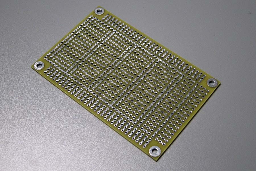
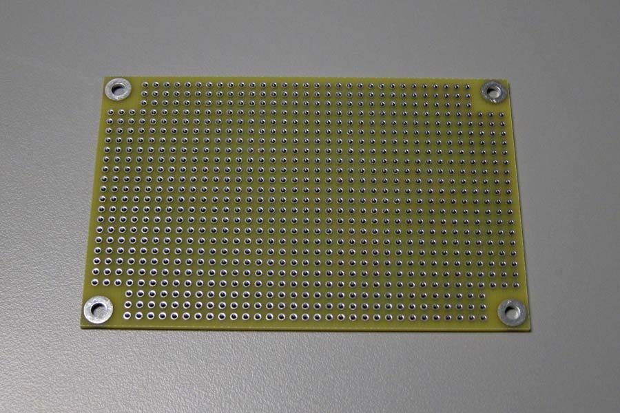
There are also some photographs of the manufactured boards (nothing fancy no solder mask or silkscreening) and pictures of the top and bottom layers. Theres also a photo of one of the boards in action.
Im not planning to mass produce or sell these boards and I thought people might be interested in the design. The expresspcb pcb file is attached if anyone wants to make one as is.
The board is sized to match the larger platform boards and, consequently, the 3 for $51 size from expresspcb (www.expresspcb.com). Unfortunately this board does not qualify for that price because it has too many holes.
Some basic features:
1) Most of the board is designed using a pretty standard breadboard-type distribution of pads and traces. The busses are available throughout the board. At one end of the board are sets of pads originally intended for creating offboard connections but they can be used for any purpose (including mounting chips). For example, it is very easy to connect breakout boards and adapters with single rows of pins to these pads. Unused platform pin pads on the long sides of the boards can also be used for this purpose. There is an extra set of connected pads running across the width of the board at this end which can be connected to either of the busses or used for distribution of other signals.
2) There are no pads specifically assigned to any of the pins from the Propeller Platform boards. This allows the board to be rotated to either orientation (with the connector end at either end of the board). The board can overhang the end of the larger platform boards and one or both ends of the other boards. This makes it easy to put tall components on the board, for example, and still be able to stack another board (smaller or overhanging the other end) on top.
3) There are two busses on the board, but they are not connected to any of the Platform pins. Short jumper wires can be used to connect the pins to the busses allowing the user to select which is positive voltage and which is ground (for example). Any supply voltage (i.e., Vin, 3.3, 5.0) can be connected. Traces can also be cut to allow the use of different voltages on different parts of the busses.
4) The traces are only on one side of the board (typically the bottom, but it can be used in either orientation). This makes it easy to cut them in order to separate sections of the busses or the connected pads.
Ive attached the expresspcb pcb file for the board. This can be loaded into their free software to make changes. This file can also be submitted to them directly to have boards manufactured. This does tie you to having expresspcb manufacture boards if you want to use this file, but the design should be easy enough to reproduce using other software.
There are also some photographs of the manufactured boards (nothing fancy no solder mask or silkscreening) and pictures of the top and bottom layers. Theres also a photo of one of the boards in action.
pcb
28K

715 x 477 - 24K
711 x 476 - 22K
713 x 477 - 16K
900 x 600 - 134K
900 x 600 - 108K
900 x 600 - 89K