

BS2 and switching regulator LT1303
 john_s
Posts: 369
john_s
Posts: 369
Theory of operation:
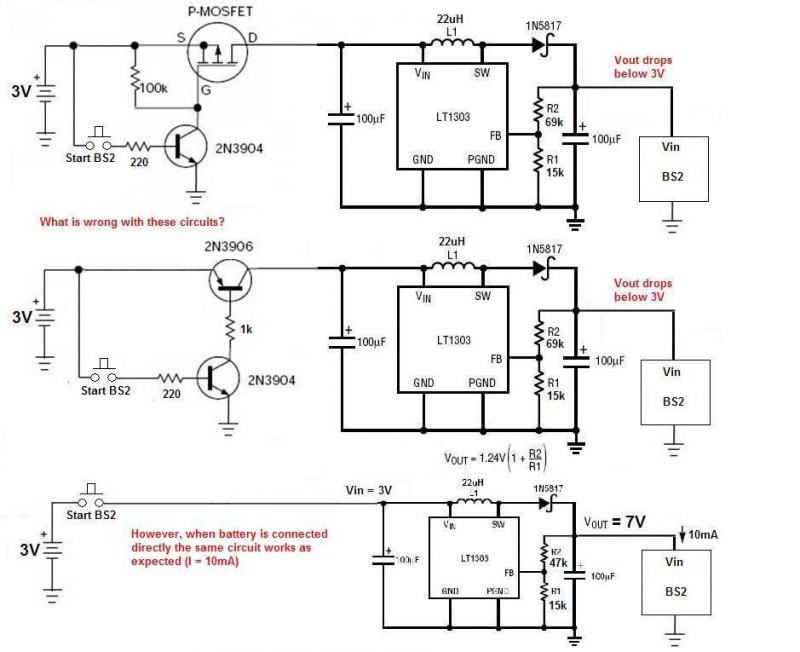
Upon the press of "START BS2" push-button the BS2 is supposed to operate from 2x1.5V = 3V batteries.
The LT1303 DC-DC converter is implemented in between the 3V battery pack and the Stamp to boost the 3V to 7V.
The bottom circuit in attached jpg proves that it works as expected.
However, (see the first 2 circuits in jpg) when placing a 2-transistor interface between a push-button and input to the DC-DC converter the LT1303 dies and does NOT supply enough voltage to BS2.
Without the BS2 load all 3 circuits perform identically, i.e. I can measure close to 7VDC at the LT1303 switcher in all three configurations.
One idea's that the PNP transistor is not driven hard enough and kills the 3V Vin to the switcher to something around 2V making it hard to generate any higher Vout. To prove otherwise I connected its Base to GND for a moment - no effect other than some heat (as expected when omitting a base to gnd resistor :-)
I must be missing something obvious...
Any advice on why the first 2 circuits do not work as expected?
800 x 652 - 57K
Comments
How about leading us through your theory of operation?
There must be a better way to isolate a 3V battery from the following booster circuit.
This circuit uses way too much current to do just that.
Any comments/ideas?
If you use a pmosfet, it will have to be a very low threshold type. "logic level", "trench" or "vertical channel" are words that go with that type. Vgs=<1Volt.
There should be a resistor of say 10kΩ from the 2N3904 base to ground. Same thing, 10kΩ from base to emitter of the '3906.
The resistor to the pushbutton (220Ω as shown on your schematic) should be more like 1 kΩ. Put the 220Ω between the collector of the '3904 and base of the '3906. Directly connecting the '3906 base to ground may have fried that transistor.
Thank you for reviewing it...
With the intention to use just 2 C-size batteries to power the BS2 I expected to come-up with the simple DC-DC solution. The disappointment came when I was loosing the battle with LT1303 and its in-rush current. In shown configuration the LT1303 still keeps shutting down when confronted with the load of around 80mA. At higher currents all I can get out of it is well below 5V and that does not even want to start the BS2. I would not even mention the battery current that I'm seeing then :-)
Yes, as you pointed out there's an additional circuitry (see attached jpg) that I omitted for simplicity.
Regards, John
You might try a beefier transistor in place of the 2N3904. For bipolar I swear by the Zetex e-line, for example the ZTX1149A is a superbeta PNP, modified TO92, pulsed Ic of 3 amps, and about 100mV in saturation with 3mA base drive and 0.5Amp collector current. A transistor like that can make a world of difference. There are nice pmosfets out there too. Are you working in thru-hole or SMT?
These are simulation curves... where BS2 is substituted with 80 Ohm load resistor (so that Vout/Rload = around 80mA)
GRN line = Vout of LT1303 shows that it reaches 6.3V at R load
BLUE line (kind of overlapping with the GRN line) proves that LT1303 is capable to deliver at least that much current i.e. close to 80mA
RED line = Vin to LT1303 as measured at collector of 2N3906
I will try Zetex line, although both old and proven 2N3904 and 2N3906 are also known for their low VCEsat below 0V3.
A switcher is all SMD on its own PCB, while the rest is mix and match - see attached some pics of my actual circuitry.
Now, why the 80mA circuit - despite its successful simulation - refuses to work with the simple switch?
However, it works perfectly without a button circuitry as seen on "80mA works only wout button.jpg"
Perhaps there's a good reason for not using any front end ON-OFF circuitry when using switchers with certain higher load current. You can find plenty of examples showing ON-OFF circuitry placed BEHIND the switcher but I yet to come with the appnote describing the same placed IN FRONT OFF the switcher.
As far as current spikes - I am sure they are all over the place during first few milliseconds as the simulation shows currents reaching 2A (!) Perhaps the strait battery acts here as a filter to those momentary spikes or shorts and has no problem handling them, while the transistor circuitry cannot cope with these states at all - and makes the switcher hard to turn on.
A 2N3906 can't supply 2A pulses. Was the transistor model worked into the LTspice simulations?
I was doing it in the past in my other design where I used SHDN pin but it still requires some in-series MOSFET to disconnect the load behind LT1303 so that it is isolated from "naked" Vbat as seen via L and the Schottky diode...
However, just before going that way I suddenly realized my mistake... so here it goes :-)
Well, after making a mistake (or was it ? ...) in answering to you I thought that I mistakenly said "12A" instead of "2A"... I realized that only after my reply went out and tried to correct it afterward. But then, it struck me that I really saw current simulated at even higher values. Sooo... what was the cause of it??? The HUGE cap in front of the switcher of course!
Way it went to be conveniently replaced with u1 SMD and voila - the circuit's alive!
Now, 100uF sits in parallel to the battery (where it supposed to be in the first place) to ease up its burden when working towards the switcher. Hats off to the basic - errr.. "..elementary my dear Watson" [ACD] :-)
p.s. thanks Tracy for steering my brain towards thinking. It took me only 2 weeks or so before I decided to look at it from other angles. Well, never too late to correct NOW obvious mistake in design... btw, I'm still waiting for the guy from LTC to come up with their answer. As soon as I get it I'll post it here as well.
I forgot about the path through the inductor and the diode. A load cutoff at the output, such as the one on page 10 of the data sheet, might do the trick too. But yours achieves a lower, near zero current.