

Low input current Half Bridge driver ...
 Beau Schwabe
Posts: 6,576
Beau Schwabe
Posts: 6,576
I wanted to throw this out in the forums for a proper litmus test.
This type of circuit seems to be popular lately ... Something for the EXPO, I needed a relatively low input current (about 1mA) to adequately drive (with at least 150mA) the gates of a couple NMOS and PMOS transistors, and I wanted the high side drive verses the low side drive to be equally balanced or at least close. In simulation I took this up to 25kHz and loaded the gate capacitance of the MOSFETs with 0.01uF ... no problems that I could tell.
If the Input is left floating, the OUTPUT defaults to being driven LOW via the hard wired 100K resistor. For opposite operation wire the 100K to GND instead.
The circuit is designed to accept TTL output where you have a 0.6V buffer on either power rail but it will work with CMOS output also.
Edit: The attached image (The lost art of perf-boarding) shows the circuit minus the MOSFETs
▔▔▔▔▔▔▔▔▔▔▔▔▔▔▔▔▔▔▔▔▔▔▔▔
Beau Schwabe
IC Layout Engineer
Parallax, Inc.
Post Edited (Beau Schwabe (Parallax)) : 6/10/2010 4:32:09 PM GMT
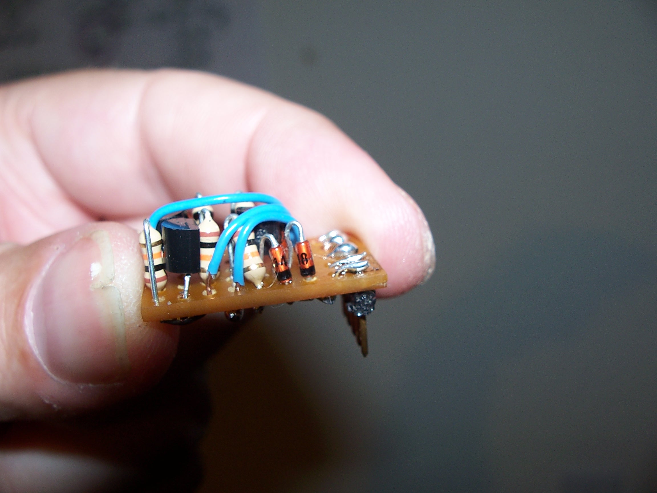
2304 x 1728 - 425K
Comments
I'm keeping it alive..lol
My projects look really good unless you
turn the boards over
I just can't justify the cost of a single custom
board as long as I can make an ugly go of it
with a piece of cheap perf board.
BTW) ...been doing some testing since my original post and this driver has worked out really well
▔▔▔▔▔▔▔▔▔▔▔▔▔▔▔▔▔▔▔▔▔▔▔▔
Beau Schwabe
IC Layout Engineer
Parallax, Inc.
The backside of that board looks really familiar to me.
It's actually harder to do the rats nest of point-to-point
wiring beneath a perf board project than it is to do sm
construction on a custom board.
In my particular application I won't be going much over 5kHz so this time I will leave it the way it is.
▔▔▔▔▔▔▔▔▔▔▔▔▔▔▔▔▔▔▔▔▔▔▔▔
Beau Schwabe
IC Layout Engineer
Parallax, Inc.
You can see where the Half bridge driver is being used, about middle of the Solderless-Bread-Board, and the two MOSFETs to the right.
Hopefully this will be 1 of about 4 things I want to demonstrate at the EXPO ... we'll see how things go if that will happen or not.
▔▔▔▔▔▔▔▔▔▔▔▔▔▔▔▔▔▔▔▔▔▔▔▔
Beau Schwabe
IC Layout Engineer
Parallax, Inc.
Is the PMOS transistor symbol flipped in your schematic?
-Phil