

Demo Shield for Propeller Platform
 Rayman
Posts: 16,458
Rayman
Posts: 16,458
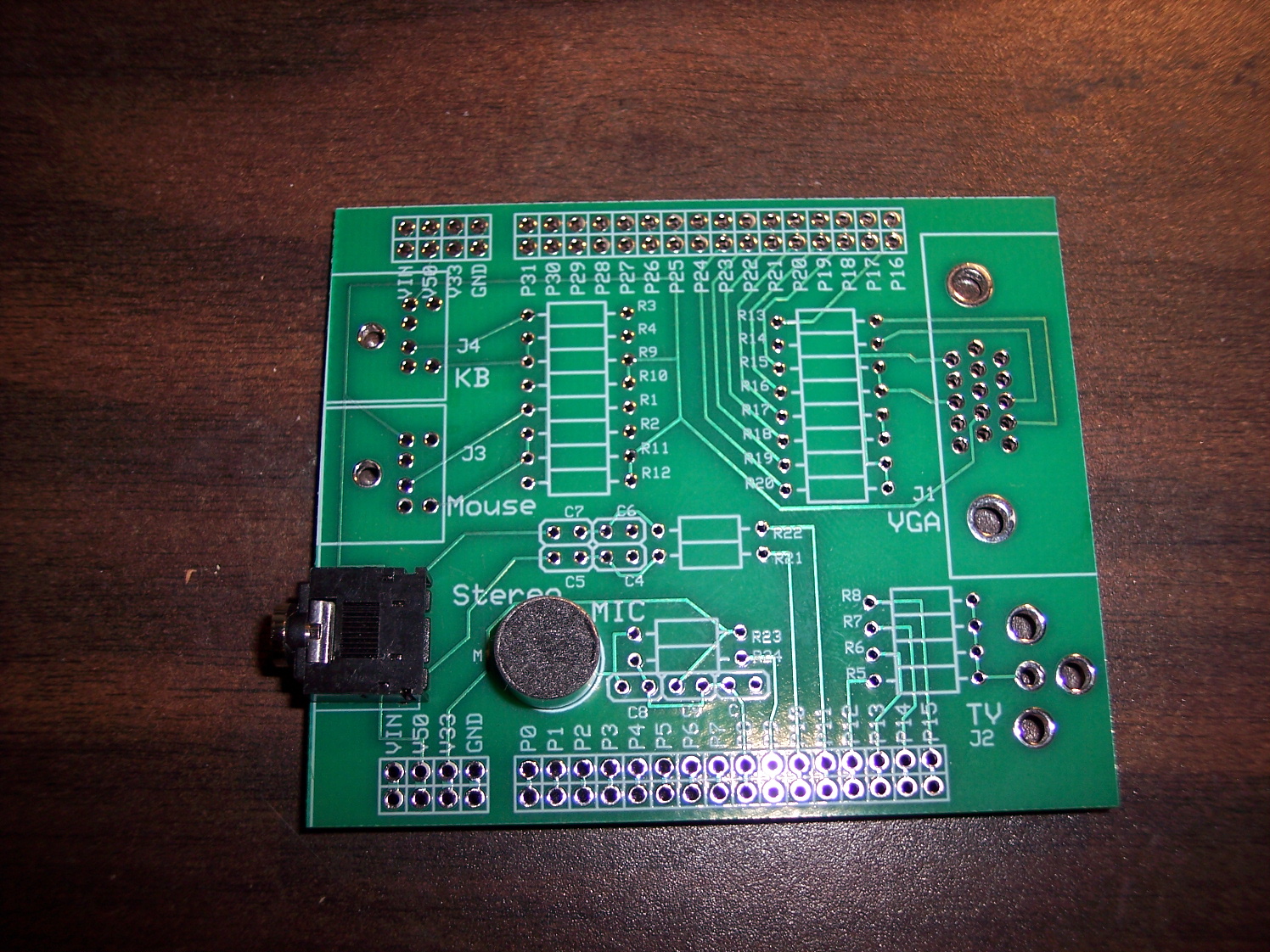
Here's my ExpressPCB design files for a VGA/TV/Keyboard/Mouse/Mic/Audio shield for the Propeller Platform.
Feel free to use them as you wish.
It has not been tested yet.
(and some have expressed skepticism about whether the microphone will work or not)
NOTE:· This design is in·a preliminary stage and is not meant to demonstrate best practices for layout or schematic!
▔▔▔▔▔▔▔▔▔▔▔▔▔▔▔▔▔▔▔▔▔▔▔▔
My Prop Info&Apps: ·http://www.rayslogic.com/propeller/propeller.htm
My Prop Products:· http://www.rayslogic.com/Propeller/Products/Products.htm
Post Edited (Rayman) : 5/15/2010 3:37:08 AM GMT

Comments
▔▔▔▔▔▔▔▔▔▔▔▔▔▔▔▔▔▔▔▔▔▔▔▔
Leon Heller
Amateur radio callsign: G1HSM
▔▔▔▔▔▔▔▔▔▔▔▔▔▔▔▔▔▔▔▔▔▔▔▔
My Prop Info&Apps: ·http://www.rayslogic.com/propeller/propeller.htm
My Prop Products:· http://www.rayslogic.com/Propeller/Products/Products.htm
Bill
▔▔▔▔▔▔▔▔▔▔▔▔▔▔▔▔▔▔▔▔▔▔▔▔
Leon Heller
Amateur radio callsign: G1HSM
That said, I do believe the board is functional, although that hasn't been proven.
I'll agree it may be lacking in the style and grace department...
▔▔▔▔▔▔▔▔▔▔▔▔▔▔▔▔▔▔▔▔▔▔▔▔
My Prop Info&Apps: ·http://www.rayslogic.com/propeller/propeller.htm
My Prop Products:· http://www.rayslogic.com/Propeller/Products/Products.htm
My business partner is a master at PCB layout and has coached me for my projects (e.g., those going to Nuts & Volts). For your consideration....
1) When laying out components, look for opportunities to introduce symmetry; it's appealing to the eye
2) Work on a standardize grid; I use 0.025 in ExpressPCB
3) (BIG ONE) Keep all traces on 90s and 45s -- avoid wonky angles because it is distracting to the eye
4) Avoid 90-degree angles in traces -- especially small ones (can cause issues in manufacturing)
There are times when we use components that have odd pin spacing and the 90s and 45s thing is not automatic with the "snap to grid" in ExpressPCB. Not a problem; simply click on the corner that is out-of-whack, hold the Shift key, and then use the arrow keys to nudge the corner into position (do this zoomed in so that you can see when a trace is on a 90 or 45).
Just for the practice I moved the traces on the top layer of your board (see attached PDF). To my eye, it looks better (a very subjective term, indeed), more professional. These little tweaks and cleanups are quick to apply and -- you may find -- will instill more confidence in potential customers.
[noparse][[/noparse]Edit] As·Phil points out this has become·a "teachable moment"·-- and useful one, I think -- I've attached the ExpressPCB file with modified with my suggestions as well as those from Phil.
▔▔▔▔▔▔▔▔▔▔▔▔▔▔▔▔▔▔▔▔▔▔▔▔
Jon McPhalen
Hollywood, CA
Post Edited (JonnyMac) : 5/14/2010 9:53:22 PM GMT
I merely provide it as a point of reference to anyone that might want to do something similar.
▔▔▔▔▔▔▔▔▔▔▔▔▔▔▔▔▔▔▔▔▔▔▔▔
My Prop Info&Apps: ·http://www.rayslogic.com/propeller/propeller.htm
My Prop Products:· http://www.rayslogic.com/Propeller/Products/Products.htm
@Rayman: Thanks for sharing - I think having an equivalent of the demo board available for the PropPlatform is a GREAT idea; especially if the user wants to check-out some of the demo stuff, or just make sure any problem they're encountering isn't down to their own module.
▔▔▔▔▔▔▔▔▔▔▔▔▔▔▔▔▔▔▔▔▔▔▔▔
Cheers,
Simon
www.norfolkhelicopterclub.com
Announcement: To cut costs in the current economic climate, we have switched-off the light at the end of the tunnel.
Apart from the layout and (no offense to leon or anyone else) other rather picky constructive advice, I suggest finding some way to get a 12x17 mini-breadboard on there as well so its function as a demo board shield is truly revealed. Maybe you could use resistor networks and possibly surface mount stuff. To make more room, what you may consider doing is swapping the positions of the mic and the stereo connections, having the stereo connected to the I/O on the bottom of the board. That way, you could get some extra room for a mini-breadboard.
Then again, this could just be a bottom-stacking module; thus nullifying the need for a mini-breadboard, and would probably work out better in the end...
▔▔▔▔▔▔▔▔▔▔▔▔▔▔▔▔▔▔▔▔▔▔▔▔
MCU Projects·- my new site where I will be posting all projects, code, etc.
Quit buying all those fixed voltage regulators, and·get an Adjustable Power Supply·for your projects!· Includes an LED testing terminal!
SD Card Adapter·- Add extra memory to your next Propeller project with ease!
More than you think. I've decided not to buy some seemingly-interesting products from some forum members because of my extreme discomfort with the PCB layout. My thought is, "If they won't take the time to do it neatly, did they take the time to actually verify that it works?" "If the layout is quick-and-dirty, is the design?" Neatness counts when you're selling something. Have a look at any of Parallax's PCBs... they always look spectacular, and work well, too.
▔▔▔▔▔▔▔▔▔▔▔▔▔▔▔▔▔▔▔▔▔▔▔▔
Jon McPhalen
Hollywood, CA
▔▔▔▔▔▔▔▔▔▔▔▔▔▔▔▔▔▔▔▔▔▔▔▔
Cheers,
Simon
www.norfolkhelicopterclub.com
Announcement: To cut costs in the current economic climate, we have switched-off the light at the end of the tunnel.
▔▔▔▔▔▔▔▔▔▔▔▔▔▔▔▔▔▔▔▔▔▔▔▔
Leon Heller
Amateur radio callsign: G1HSM
Post Edited (Leon) : 5/14/2010 8:10:21 PM GMT
I'm with Jon: a good layout should have an aesthetic resonance to it. I like to call it the "feng shui" of PCB design.
-Phil
▔▔▔▔▔▔▔▔▔▔▔▔▔▔▔▔▔▔▔▔▔▔▔▔
My Prop Info&Apps: ·http://www.rayslogic.com/propeller/propeller.htm
My Prop Products:· http://www.rayslogic.com/Propeller/Products/Products.htm
http://www.alternatezone.com/electronics/files/PCBDesignTutorialRevA.pdf
He does mention symmetry and avoiding right angles, but says that these are just for appearance...
I do think it's a good idea to use symmetry and 45-degree only angles for boards that people will see.
But, I think it the real world, the traces are hidden deep inside a multilayer board where no one can see them.· Plus, they're inside a case and never see the light of day.· I don't think the iPhone PCB designers worries too much about symmetry!
I as still unconvinced of any bad effects of right angle bends.· I think their avoidance is a throw back to old days of low quality production techniques...· The above guide also says that any EMI problems are myth.· Still, I avoid them just for appearance sake.· I just sent an email to expresspcb support to see if their really are concerns about manufacturing quality of right angles...
▔▔▔▔▔▔▔▔▔▔▔▔▔▔▔▔▔▔▔▔▔▔▔▔
My Prop Info&Apps: ·http://www.rayslogic.com/propeller/propeller.htm
My Prop Products:· http://www.rayslogic.com/Propeller/Products/Products.htm
Post Edited (Rayman) : 5/15/2010 12:22:28 PM GMT
My understanding of the right-angle thing is that the outer corner can become beveled in etching which reduces the effective trace width at that point, so the "avoid right angles" thing is really important for very small traces. As "practice makes permanent" it just becomes a good habit to stick to 45s when bending traces of any size.
▔▔▔▔▔▔▔▔▔▔▔▔▔▔▔▔▔▔▔▔▔▔▔▔
Jon McPhalen
Hollywood, CA
Post Edited (JonnyMac) : 5/15/2010 2:06:23 PM GMT
You said "I as still unconvinced of any bad effects of right angle bends."
One of problems on that in real world is - TOP of that angle have mechanical problems to hold to PCB (Very sensitive to bend it out of PCB).
Regards
ChJ
▔▔▔▔▔▔▔▔▔▔▔▔▔▔▔▔▔▔▔▔▔▔▔▔
Nothing is impossible, there are only different degrees of difficulty.
For every stupid question there is at least one intelligent answer.
Don't guess - ask instead.
If you don't ask you won't know.
If your gonna construct something, make it·as simple as·possible yet as versatile as posible.
Sapieha
▔▔▔▔▔▔▔▔▔▔▔▔▔▔▔▔▔▔▔▔▔▔▔▔
Leon Heller
Amateur radio callsign: G1HSM
Post Edited (Leon) : 5/15/2010 3:00:02 PM GMT
Restrictive conventions such as limiting angles to 0,90, and 45 have a sound basis in EM theory for the 45s provided they are crossing with a dialectic layer between them , not parallel. When I was an auto mechanic some types of miss-fire could be cured just by rerouting the plug wires so they crossed each other at 90 degree angles. Conversely there are designs where the sharp 90 degree angles are essential for the design. In Temp, AZ NELTEC makes the boards that cell phone antennas are etched into. The frequencies involved rule out fiberglass so the use a PTFE type laminate. The antenna design didn't even exist back in my ham days. Its called a fractal antenna. It consists of many square corners and boxes required by fractal equations. Apparently this allows a wide frequency range with good gain over the band. Since we don't want our boards "transmitting" we avoid 90 degree traces for reasons other than just etching chemistry alone. There is way too much theory in this post so I've up-loaded an attachment that demonstrates a smooth transition from .8 mm to .025" trace pitch. I hope to demo this board's app at UPEW. Yes Leon, I'm double checking the schematic as I post.
▔▔▔▔▔▔▔▔▔▔▔▔▔▔▔▔▔▔▔▔▔▔▔▔
MOORE'S LAW: The capabilities of electronics shall double every 18 months.
cloyd's corollary: Hardware is easy, software is hard.
Post Edited (yarisboy) : 5/18/2010 1:35:09 AM GMT
Here's what they say:
When placing narrow traces, 0.015" or less, avoid sharp right angle turns. The problem here is that in the board manufacturing process, the outside corner can be etched a little more narrow. The solution is to use two 45 degree bends with a short leg in between.
Fortunately, the smallest trace I use is 0.020".· Still, I will try to be more feng shui in the future and use only 45 degree turns...
▔▔▔▔▔▔▔▔▔▔▔▔▔▔▔▔▔▔▔▔▔▔▔▔
My Prop Info&Apps: ·http://www.rayslogic.com/propeller/propeller.htm
My Prop Products:· http://www.rayslogic.com/Propeller/Products/Products.htm