

High Current DUAL LDO Design for PROPELLER Board , Please Comment
 DavidM
Posts: 640
DavidM
Posts: 640
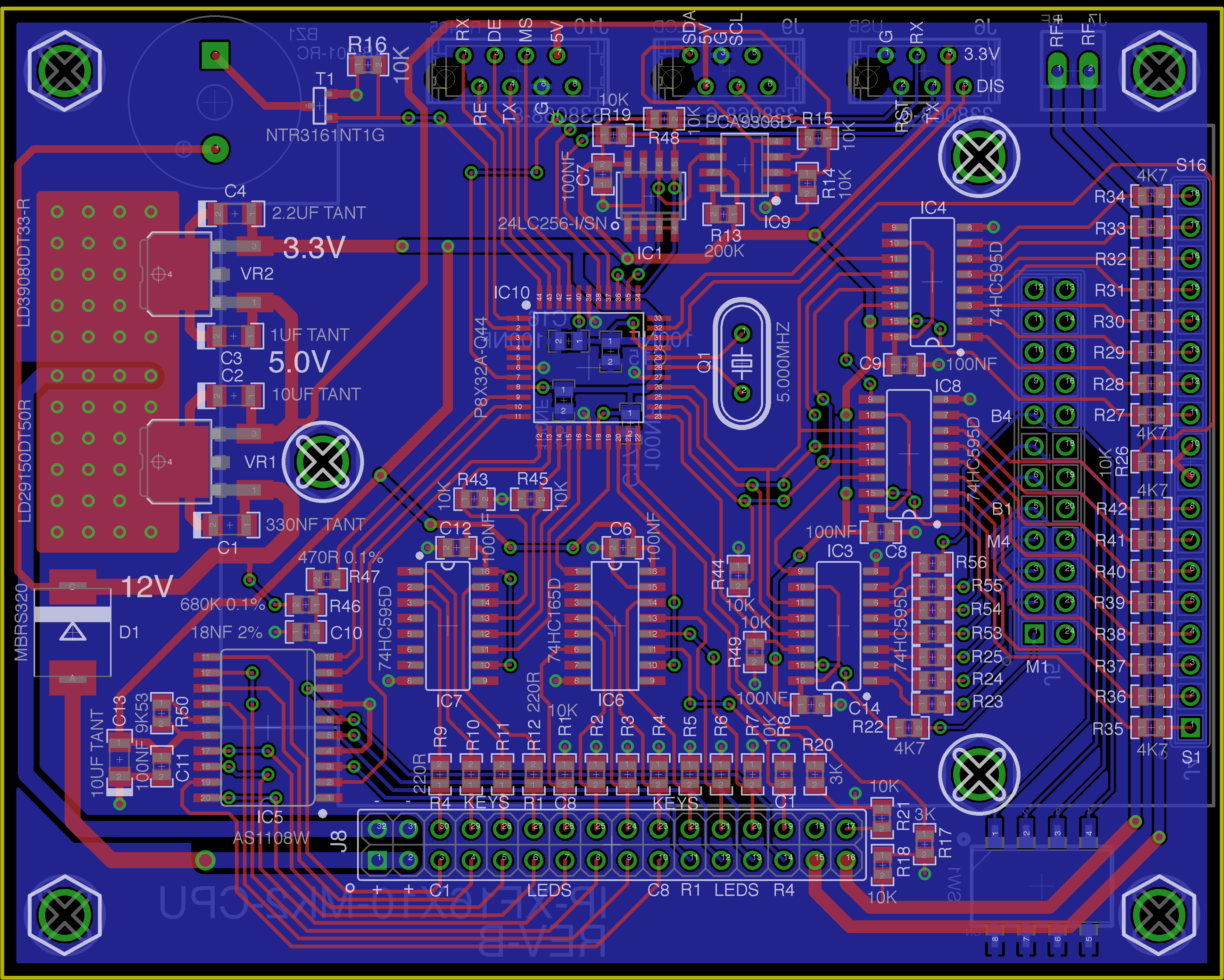
HI,
This is my current design ( My first SMD version) of a motherboard that uses the prop chip which uses 2 LDO' regulators ( 5V & 3.3V) Instead of a Switching Regulator ( that I normally use) , I have utilised a PCB Copper/Fill as a "HEAT SINK".
I do have some design constraints as follows..
P1) I have a height restriction of 10mm on the component side.
P2) I have an RF Transmitter board ( 900mhz 65mW) attached to the SOLDER SIDE of this board. It was recommended by the designer of the RF Transmitter Board not to use a SWITCHING POWER SUPPLY, as the Power supply components are right next to the RF Output circuitry, even thought its on the opposite side.
P3) My board runs of a 12V SLA Battery, Efficiency is not a requirement in this design ( I know switching power supplies are much more efficient)
P4) This board will should not require any more than 500ma of power at the most, but this board will need to handle more in a future design.
I will be printing the component values only for the first few prototype boards ( the production boards will not have this)
So, MY QUESTIONS ARE...
Q1) Will my "HEATSINK" design be adequate ? I can make more area if need be. I don't have room for a "REAL" Heatsink.
Q2) Have I positioned and connected the Input & Output Capacitors correctly for the regulators.
Q3) I have noticed recently some posts regarding de-coupling caps for the prop, I have utilised 4 on the Solder Side.
I have attached a full schematic ( with components part numbers ) and a full hires PCB layout drawing.
You can comment on any other parts of the design if you wish, but I am not too concerned about this at the moment ( unless you see a show stopper!)
Thanks
Dave M

3524 x 2821 - 478K
Comments
It would seem a wise precaution to add the best heatsinking/heatspreading that you can to both
sides of the board: any reason not to bond/bolt some thick aluminium or plated-copper sheeting to the
regulators?
You can get metal-cored PCB's now - they're mighty expensive 'though ...
Regards,
T o n y
www.eurocircuits.com/index.php/New-services/IMS-pool-our-new-special-application-PCB-prototype-service.html
▔▔▔▔▔▔▔▔▔▔▔▔▔▔▔▔▔▔▔▔▔▔▔▔
Leon Heller
Amateur radio callsign: G1HSM
I can move the 3 volt regulator closer to the prop chip, this would then give me more area of copper,
Should I MASK around the revers side, the whole back layer is a ground plane, but will the masking prevent heat dissipation?
PS,
I read somewhere that any more than 1 inch square of copper ( as a heatsink) makes no more improvements to heat dissipation, But somehow I don't believe that!
thanks
Dave M
A nice thick, big chunk of appropriate metal gets the heat away from the chips and spreads it: which
is always a good start.
Obviously you still need to get rid of the heat at the average rate that it's being produced, or the
temperature of the heatsink will rise and rise and rise ... ignore this at your peril.
In the simplest terms, let's say that your linear voltage-droper produces 6W of heat. Now google
6W heatsinks to get some idea of the scale of the problem, and make sure that your enclosure
solution is capable of coping: I've used small blowers ~ 6mm thick where I couldn't fit anything more
sensible. And always an aluminium box, because cool is best!
Regards,
T o n y
The proper way to determine optimum heatsink size involves an insane amount of math and in many cases is not necessary unless thermal management is the number one concern of your design. After looking at your circuit layout, schematic, and your notes, this is not the issue. (By the way, your board is laid out very well!) Using copper pours/ground planes as a heatsink is the solution for your design. In regards to your layout, as depicted in your screenshot, I don't believe you will have any issues with heat from your 500mA total draw. It appears the heatsink area on the tops side is tied to the ground plane on the bottom?
Other options to consider if you are still concerned:
1) You can increase the diameter of your vias to gain additional surface area of your "heatsink" and to allow for some natural convection effects.
2) You can specify a heavier copper thickness for one or both sides of your board. I have seen many boards that will increase from teh 1/2oz typical copper to a 1 oz copper thickness for boards with thermal concerns. I have also seen a board with six 3 watt RGB LEDs that was 2oz copper on all 4 layers to dissipate the heat generated.
I didn't see any application notes regarding thermal design on the ST site for either of these parts. There is an L200 regulator appnote that has some good pointers that can be utilized for this regulator in regards to thermal management.
For future designs (you mentioned a higher current need down the road), I would look into utilizing the TO-220 package since it has better thermal properties. You can mount it laying down to get under the 10mm requirement.
▔▔▔▔▔▔▔▔▔▔▔▔▔▔▔▔▔▔▔▔▔▔▔▔
Andrew Williams
WBA Consulting
WBA-TH1M Sensirion SHT11 Module
Special Olympics Polar Bear Plunge, Mar 20, 2010
1) isolate ground plane connecting to main ground plane only on layer below traces runing acrose isolation region.
2) place all parts on 1 side
3) use ground plane(As best as possible) on both sides and for sure surounding entire circuit
4) leave outer ring of top ground plane uncovered by solder mask
5) get an aluminimum box bent to fit over switching supply that can be soldered to ground ring.
this should prevent any interference. though unless you have metal working tools or are making lots step 5 may get expensive.
▔▔▔▔▔▔▔▔▔▔▔▔▔▔▔▔▔▔▔▔▔▔▔▔
Check out my brand new site.
▔▔▔▔▔▔▔▔▔▔▔▔▔▔▔▔▔▔▔▔▔▔▔▔
Leon Heller
Amateur radio callsign: G1HSM
TO-3 packages cost more, but they're tough and·these shred, especially the thermal stress.· A 7805, TO-3, the case is still Ground; bolt it to the copper (GND plane)·on one side,·and·its input and output on the other·side with·relieved pads.· Beyond that, for it to totally rock, I'd heatsink it, but in this case I think that's optional.
Rich H
▔▔▔▔▔▔▔▔▔▔▔▔▔▔▔▔▔▔▔▔▔▔▔▔
The Simple Servo Tester, a kit from Gadget Gangster.
Thanks for all the replies!
I have made my "HEATSINK" area as large as I can, I moved the diode down , and the 3.3v regulator across to the right. I also changed the GND trace.
I made the vias much bigger and used more of them.
The TOP HEATSINK IS connected to the BACK LAYER GROUND PLANE, and this heatsink has a solder mask . I will probably go for GOLD PLATING.
I am going to go with this design and see how it runs, I think my current requirement is low for this version, In a future version I will use a switching power supply, ( I know how to do that ).
The 5v regulator has current limit & thermal shutdown, so I should be save.
This job has its design restrictions, I.e the HIGHT RESTRICTION and the RF MODULE being close, I cannot change this, so I need to try the LDO regulators out.
I might try out a thicker copper as well.
I have attached an updated drawing.
Thanks for everyones comments! especially ANDREW WILLIAMS
Dave M
That mounting hole is close, but I always use a plastic(nylon) washer, and I have made the SILK a little bigger than the head of the M3 Screw, So It should be ok,
Thanks for pointing that out!
Dave M