I am under the impression at this point that the gate voltages need to be higher. I cant seem to come up with a clever way to use the propellers voltage to drive the MOSFETs. Perhaps a comparator a transistor. Hum...
▔▔▔▔▔▔▔▔▔▔▔▔▔▔▔▔▔▔▔▔▔▔▔▔
"Carpe Ducktum" "seize the tape!!" peterthethinker.com/tesla/Venom/Venom.html
Never underestimate the bandwidth of a station wagon full of tapes hurtling down the highway. —Tanenbaum, Andrew S.
LOL
Post Edited (Peter KG6LSE) : 12/10/2009 4:40:02 PM GMT
@ Peter KG6LSE
Yes i am aware of the ICs that can do what I am trying to do. This is all for education as I want to use and learn more about the mosfets. Thanks for the suggestions.
@ PJ Allen
Could you elaborate on the logic level thing. When looking at the data sheet for a mosfet is this called the gate to source voltage? Also what is V_s and V_g?
Zap-o, PJ is basically correct in what he says. Q2 and Q4 may conduct slightly with a 3.3 or 5V level on the gate but they need 10V to turn on fully. Q1, Q3, and the PWM transistor would need at least 10V and probably more to conduct fully.
Peter and Loopy also have good points. Normally the bottom pair would be N channel and the top P channel transistors, and the PWM signal would be part of the gate drive signal.
Also, nowhere does it say which inputs you're driving in the circuit. In this setup driving the wrong inputs with the wrong signal can result in a direct short.
"I am under the impression at this point that the gate voltages need to be higher. I cant seem to come up with a clever way to use the propellers voltage to drive the MOSFETs."
The voltage that needs to be supplied across the gates, can not be achieved by simply driving the gate's higher with reference to your ground. The gates need to have at least 10V between each of the Gate-Source. Q4 or Q2 will have no problem turning on, its any of the others that will have an issue.
Take for example Q2, if it's "on" and you want to turn on "Q3" by placing 10V on C, the only way that it will turn on is if your load has a relatively low resistance (which is why you may not be seeing any results). The reason is that in order for it to come on you also need 10V across the Gate-Source. The only way for the source of Q3 to see your ground reference is through your load and Q2 when it is on. The result is that you will only see about a bandgap of voltage across your load. ... About 0.6V The same scenario for the PWM mosfet, only it will be severely in it's linear operating mode and if you are able to pass any amount of current, this will be where you get most of your heat, and probably damage the mosfet. The same is also true if the PWM mosfet were eliminated and Vin was applied to Q1 and Q3's Drain. It would be one of those two transistors getting very HOT.
As it has been indicated, typically you have a complementary pmos transistor towards the top of the rail, however this does not always have to be the case. Sometimes, usually for better matching characteristics you might want an all n-mos H-Bridge or an all p-mos H-Bridge. This is perfectly valid, but it requires a special driver and special considerations.
The solution that Peter KG6LSE posted is exactly what you need. You can eliminate the PWM mosfet in your design by applying PWM to one of the legs on the H-Bridge instead of keeping it steady.
▔▔▔▔▔▔▔▔▔▔▔▔▔▔▔▔▔▔▔▔▔▔▔▔ Beau Schwabe
IC Layout Engineer
Parallax, Inc.
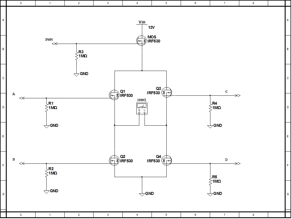
Thanks far for all the help. I am learning mucho. I have taken some of the wisdom in this thread and came up with this circuit. Please review and let me know the flaws....
My question now is why do some of the complementary Mosfets have a higher current rating on the P side vs N side. Is this because the current is used up driving out the Drain?
@Phil Pilgrim (PhiPi)
1. I see that the pMosfets are backwards my software is messing it up - thanks.
2. I have the B and C inputs tied low so that when the transistor is turned on by the propeller the 12Volts will be present. This still seems a problem? Could you check again please.
3. I want the IRF540 to get hot. I will heat sink it. My Idea is to completely turn on Q1 and Q2 to set direction. Then in a remote place in a case I will bolt on the IRF540 with heat sink. This is my effort to keep the heat directed away from the electronics board. Q1 and Q2 should generate little heat if fully on right?
2. What I said is correct. The emitter of an NPN transistor is always at least 0.6V lower than the base. An emitter follower can never source more voltage than its base input provides. Use a proper MOSFET driver.
4. I think you're making a mistake trying to adjust speed linearly. A MOSFET is highly nonlinear and will not provide the smooth control you expect. Moreover, there will be temperature dependencies that make such an arrangement unreliable. Finally, adding a voltage drop below the H-bridge makes it all that much harder to drive the nMOSFET legs effectively. If you PWM the nMOSFET legs instead, all these problems go away, and your system will run cool.
#2
Q6 and Q7 are going to have similar problems that your Q1 and A3 mosfets had in your original design. As they are this is an improper configuration of the NPN transistors and they will only be capable of delivering about 2.75V to the gates of your nmos transistors. Instead, Q6 and Q7 should be PNP transistors ... If this sounds familiar, there is a reason, the same was true with the nmos verses the pmos transistors. ( I have attached a schematic that should work for the nmos gate drive)
R5 and R6 should be something smaller like 1K.
#3
Why on earth would you want the transistor to purposefully get hot? - That is a flawed design practice. HEAT equals energy that you can either conserve in your available battery life, or direct as much as you possibly can to your motor. In order to do the latter of the two, you need to completely turn the nmos and pmos transistors on in the direction you want the motor to go. ... if anything the only thing that should be getting warm is your motor. ... for instance, I have an AC-Power-Inverter design that I am working on that draws about 40 Amps... The transistors are cool to the touch, what's warm is the transformer. It's warm, because the secondary coils have too much resistance and under a load they generate heat but the ratio between the primary and secondary are correct. In this case what I would need to do is lower the number of turns on the primary as well as the secondary while keeping the same ratio. This effectively would reduce my 'resistive' heating in the transformer, and allow me deliver more power to my load. I mention this because a very similar thing happens with a mosfet that is not fully turned on. It will operate in it's linear region and act very much like a resistor in turn generating HEAT and wasting energy when it could by design be completely avoided. This is also why the Rds "ON" value is so important with a mosfet when driving high current loads.
Note: Since you are driving an inductive load (i.e. a motor) and even though the transistors have a built-in reverse diodes, it is a wise idea to provide additional diode protection to your transistors and NOT rely on the bulk diode inside the transistor.
▔▔▔▔▔▔▔▔▔▔▔▔▔▔▔▔▔▔▔▔▔▔▔▔ Beau Schwabe
IC Layout Engineer
Parallax, Inc.

 Zap-o
Posts: 452
Zap-o
Posts: 452

Comments
In this case, I suspect Q2 ans Q4 are wrong.
▔▔▔▔▔▔▔▔▔▔▔▔▔▔▔▔▔▔▔▔▔▔▔▔
Ain't gadetry a wonderful thing?
aka G. Herzog [noparse][[/noparse] 黃鶴 ] in Taiwan
I am under the impression at this point that the gate voltages need to be higher. I cant seem to come up with a clever way to use the propellers voltage to drive the MOSFETs. Perhaps a comparator a transistor. Hum...
there are H-Bridge driver chips out there .. the Main issue is going to be driving Q1 and Q3 as you Need to drive em hard .
This Might help ...
rds.yahoo.com/_ylt=A0geu6dHIyFL2rcADJBXNyoA;_ylu=X3oDMTEzMjZoczhtBHNlYwNzcgRwb3MDOARjb2xvA2FjMgR2dGlkA0Y3NTVfMTI2/SIG=12d5a40rg/EXP=1260549319/**http%3a//www.parallax.com/dl/docs/cols/nv/vol2/col/nv52.pdf
Peter ...
▔▔▔▔▔▔▔▔▔▔▔▔▔▔▔▔▔▔▔▔▔▔▔▔
"Carpe Ducktum" "seize the tape!!"
peterthethinker.com/tesla/Venom/Venom.html
Never underestimate the bandwidth of a station wagon full of tapes hurtling down the highway. —Tanenbaum, Andrew S.
LOL
Post Edited (Peter KG6LSE) : 12/10/2009 4:40:02 PM GMT
First, since your Q1 and Q3 are configured as source follower,·V_s will approximate V_g.
Second, those are IRF transistors and may not do well with "logic" level (5V) V_g.
Yes i am aware of the ICs that can do what I am trying to do. This is all for education as I want to use and learn more about the mosfets. Thanks for the suggestions.
@ PJ Allen
Could you elaborate on the logic level thing. When looking at the data sheet for a mosfet is this called the gate to source voltage? Also what is V_s and V_g?
Peter and Loopy also have good points. Normally the bottom pair would be N channel and the top P channel transistors, and the PWM signal would be part of the gate drive signal.
Can someone briefly explain what RDs(on) is? I found a Mosfet with a RDS(on) at 4.5Volts?
You want Rds(on) to be as low as possible if driving high current loads.
International Rectifier and Motorola usually have some good white-papers on their websites which help explain the basics of the products they sell.
▔▔▔▔▔▔▔▔▔▔▔▔▔▔▔▔▔▔▔▔▔▔▔▔
Tom Sisk
http://www.siskconsult.com
·
▔▔▔▔▔▔▔▔▔▔▔▔▔▔▔▔▔▔▔▔▔▔▔▔
Chris Savage
Parallax Engineering
50 72 6F 6A 65 63 74 20 53 69 74 65
·
"I am under the impression at this point that the gate voltages need to be higher. I cant seem to come up with a clever way to use the propellers voltage to drive the MOSFETs."
The voltage that needs to be supplied across the gates, can not be achieved by simply driving the gate's higher with reference to your ground. The gates need to have at least 10V between each of the Gate-Source. Q4 or Q2 will have no problem turning on, its any of the others that will have an issue.
Take for example Q2, if it's "on" and you want to turn on "Q3" by placing 10V on C, the only way that it will turn on is if your load has a relatively low resistance (which is why you may not be seeing any results). The reason is that in order for it to come on you also need 10V across the Gate-Source. The only way for the source of Q3 to see your ground reference is through your load and Q2 when it is on. The result is that you will only see about a bandgap of voltage across your load. ... About 0.6V The same scenario for the PWM mosfet, only it will be severely in it's linear operating mode and if you are able to pass any amount of current, this will be where you get most of your heat, and probably damage the mosfet. The same is also true if the PWM mosfet were eliminated and Vin was applied to Q1 and Q3's Drain. It would be one of those two transistors getting very HOT.
As it has been indicated, typically you have a complementary pmos transistor towards the top of the rail, however this does not always have to be the case. Sometimes, usually for better matching characteristics you might want an all n-mos H-Bridge or an all p-mos H-Bridge. This is perfectly valid, but it requires a special driver and special considerations.
The solution that Peter KG6LSE posted is exactly what you need. You can eliminate the PWM mosfet in your design by applying PWM to one of the legs on the H-Bridge instead of keeping it steady.
▔▔▔▔▔▔▔▔▔▔▔▔▔▔▔▔▔▔▔▔▔▔▔▔
Beau Schwabe
IC Layout Engineer
Parallax, Inc.
Thanks far for all the help. I am learning mucho. I have taken some of the wisdom in this thread and came up with this circuit. Please review and let me know the flaws....
My question now is why do some of the complementary Mosfets have a higher current rating on the P side vs N side. Is this because the current is used up driving out the Drain?
1. The pMOSFETs in your schematic are upside down.
2. Your B and C inputs will not work from logic levels.
3. With 10K pullups/pulldonws, the MOSFETs will not turn off very fast, and you risk getting shoot-through when you change motor directions.
4. The speed input will not give you a linear response, and the IRF540 is going to get hot. It would be better to PWM the B and C inputs.
MOSFET drivers, like the MIC4469, are readily obtainable and would make your job a lot easier. They would completely fix issues 2 and 3.
-Phil
Post Edited (Phil Pilgrim (PhiPi)) : 12/11/2009 10:05:14 PM GMT
1. I see that the pMosfets are backwards my software is messing it up - thanks.
2. I have the B and C inputs tied low so that when the transistor is turned on by the propeller the 12Volts will be present. This still seems a problem? Could you check again please.
3. I want the IRF540 to get hot. I will heat sink it. My Idea is to completely turn on Q1 and Q2 to set direction. Then in a remote place in a case I will bolt on the IRF540 with heat sink. This is my effort to keep the heat directed away from the electronics board. Q1 and Q2 should generate little heat if fully on right?
Again thanks for the reply.
4. I think you're making a mistake trying to adjust speed linearly. A MOSFET is highly nonlinear and will not provide the smooth control you expect. Moreover, there will be temperature dependencies that make such an arrangement unreliable. Finally, adding a voltage drop below the H-bridge makes it all that much harder to drive the nMOSFET legs effectively. If you PWM the nMOSFET legs instead, all these problems go away, and your system will run cool.
-Phil
#2
Q6 and Q7 are going to have similar problems that your Q1 and A3 mosfets had in your original design. As they are this is an improper configuration of the NPN transistors and they will only be capable of delivering about 2.75V to the gates of your nmos transistors. Instead, Q6 and Q7 should be PNP transistors ... If this sounds familiar, there is a reason, the same was true with the nmos verses the pmos transistors. ( I have attached a schematic that should work for the nmos gate drive)
R5 and R6 should be something smaller like 1K.
#3
Why on earth would you want the transistor to purposefully get hot? - That is a flawed design practice. HEAT equals energy that you can either conserve in your available battery life, or direct as much as you possibly can to your motor. In order to do the latter of the two, you need to completely turn the nmos and pmos transistors on in the direction you want the motor to go. ... if anything the only thing that should be getting warm is your motor. ... for instance, I have an AC-Power-Inverter design that I am working on that draws about 40 Amps... The transistors are cool to the touch, what's warm is the transformer. It's warm, because the secondary coils have too much resistance and under a load they generate heat but the ratio between the primary and secondary are correct. In this case what I would need to do is lower the number of turns on the primary as well as the secondary while keeping the same ratio. This effectively would reduce my 'resistive' heating in the transformer, and allow me deliver more power to my load. I mention this because a very similar thing happens with a mosfet that is not fully turned on. It will operate in it's linear region and act very much like a resistor in turn generating HEAT and wasting energy when it could by design be completely avoided. This is also why the Rds "ON" value is so important with a mosfet when driving high current loads.
Note: Since you are driving an inductive load (i.e. a motor) and even though the transistors have a built-in reverse diodes, it is a wise idea to provide additional diode protection to your transistors and NOT rely on the bulk diode inside the transistor.
▔▔▔▔▔▔▔▔▔▔▔▔▔▔▔▔▔▔▔▔▔▔▔▔
Beau Schwabe
IC Layout Engineer
Parallax, Inc.