

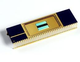
Melting memory chips in mass production
 HollyMinkowski
Posts: 1,398
HollyMinkowski
Posts: 1,398
The Article said...
South Korean manufacturer Samsung Electronics announced this week that it has begun mass production of a new kind of memory chip that stores information by melting and freezing tiny crystals.
the smaller each crystal cell in the device, the faster it becomes. Wuttig's group has recently conducted experiments with cells just 20 nanometres across. These cells can be switched in just 16 nanoseconds
Proponents hope that PCM could eventually take a substantial share of the flash memory market, worth more than $20 billion in 2008.
the technology is developing quickly, and given the advantages of PCM and the increasing difficulties of shrinking flash, Atwood says that he thinks crystal memory will become commonplace in just a few years. "We believe it is the next generation,"
www.nature.com/news/2009/090925/full/news.2009.951.html
▔▔▔▔▔▔▔▔▔▔▔▔▔▔▔▔▔▔▔▔▔▔▔▔
"Where am I? Where am I going? Why am I in a handbasket?"
Comments
▔▔▔▔▔▔▔▔▔▔▔▔▔▔▔▔▔▔▔▔▔▔▔▔
Ain't gadetry a wonderful thing?
aka G. Herzog [noparse][[/noparse] 黃鶴 ] in Taiwan
growth would lead to a shift in the interface by only 2 nm in 10 yr" the total samples were >20 nm so that would mean that over a 10 year period the high resistance area would reduce in resistance by only a fraction.