Best practice Power/Ground on Propeller Chip
 Jeff Martin
Posts: 762
Hi,
During yesterday's webinar with Chip, the topic came up that our belief as to what is causing the rare PLL burn-out failures has to do with unwanted electrical potentials created by a custom Propeller board's·layout connections, or lack thereof.·
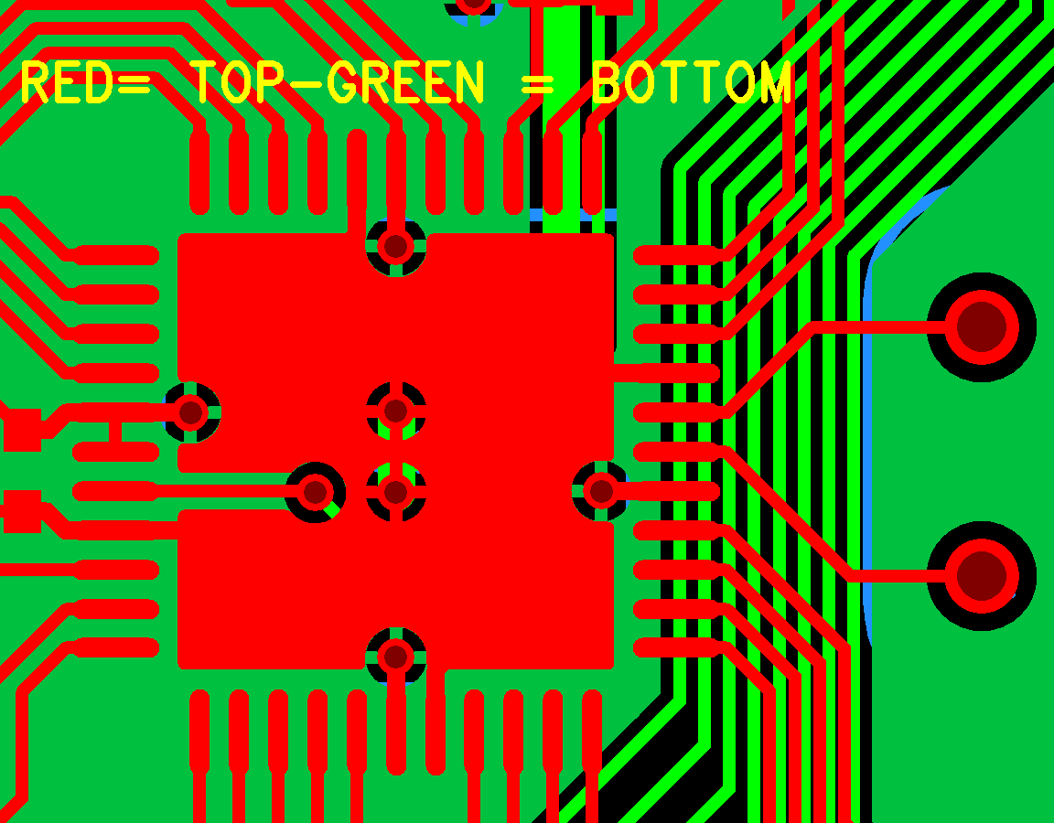
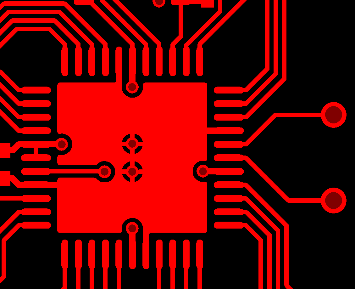
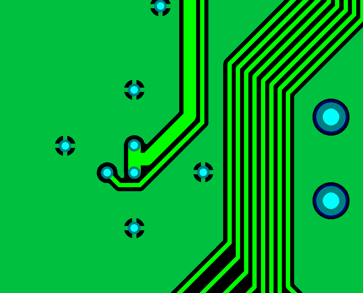
We have not been able to prove this theory, but we have also not witnessed this failure on the Propeller Demo board.· So we thought we'd share the attached images of the layout for the Propeller Demo Board as a "best practice" reference for future Propeller board/circuit designs.
Thanks.
▔▔▔▔▔▔▔▔▔▔▔▔▔▔▔▔▔▔▔▔▔▔▔▔
--Jeff Martin
· Sr. Software Engineer
· Parallax, Inc.
Post Edited (Jeff Martin (Parallax)) : 3/19/2009 6:46:15 PM GMT


Comments
Finally, on the QFN chip, which does have a center pad, won't there be another solution? The ground vias under its center pad don't seem correct.
Post Edited (Fred Hawkins) : 3/19/2009 8:52:32 AM GMT
In the design that I have done I have done something similar, but I made the center pour area be VSS (GND) and the smaller traces be VDD. But of course this is a nice looking layout because the GND plane/copper pour on the bottom layer. Interesting how this is different, inspiring some too.
What does the Propeller Protoboard layout look like compared to this?
▔▔▔▔▔▔▔▔▔▔▔▔▔▔▔▔▔▔▔▔▔▔▔▔
Timothy D. Swieter, E.I.
www.brilldea.com - Prop Blade, LED Painter, RGB LEDs, 3.0" LCD Composite video display, eProto for SunSPOT
www.tdswieter.com
But I'm not an IC design expert, so this is just speculation on my part.
-Phil
This is my pictures for.
Reconstructed ProtoBoard for stablity with 14 MHz crystal
▔▔▔▔▔▔▔▔▔▔▔▔▔▔▔▔▔▔▔▔▔▔▔▔
Nothing is impossible, there are only different degrees of difficulty.
For every stupid question there is at least one intelligent answer.
Don't guess - ask instead.
If you don't ask you won't know.
If your gonna construct something, make it·as simple as·possible yet as versatile as posible.
Sapieha
Post Edited (Sapieha) : 3/19/2009 6:57:21 AM GMT
I think what Chip said in the webinar (soon it will be on video and we can confirm) is that he thought is was something that was stressed and broken in the interface logic to the PLL. Chip said that he didn't think the PLL itself broke, but the interface logic to it.
Your reasoning on power distribution makes sense too. It would be neat to dissect a chip that has had this happen and see what is found.
▔▔▔▔▔▔▔▔▔▔▔▔▔▔▔▔▔▔▔▔▔▔▔▔
Timothy D. Swieter, E.I.
www.brilldea.com - Prop Blade, LED Painter, RGB LEDs, 3.0" LCD Composite video display, eProto for SunSPOT
www.tdswieter.com
I was a little harsh on Nick McClick when I warned him that he better ground both ground pins in his Propeller reference board kit; I didn't know about this problem, but recommended it just from general principle. Looks like I wasn't crying wolf after all!
The DIP has only two Vdd/Vss pairs, contrasted with four for the SMT packages. In the PropStick Kit (which I designed), Vss is a groundplane on the component side; Vdd, a 50-mil trace on the solder side. There is one 10uF filter cap (tantalum) and two 0.1uF bypass caps: one for the Prop/EEPROM, and one for the MAX3232. Had there been room, I'd have added another for the Prop. Attached is the board layout.
In my current work with the SMT part, I use two 1uF ceramic bypass caps on opposite sides of the chip, and both power and ground planes underneath the chip, similar to the layout Jeff posted.
-Phil
What is the corresponding best practice for the QFN prop chip?
Can I arbitrarily use the center pad as either ground or vdd?
Not quite the answer I was looking for, but it'll do for now.