

Using MCP3001 a Microchip 10-bit A/D converter with BS2
 po2le
Posts: 76
po2le
Posts: 76
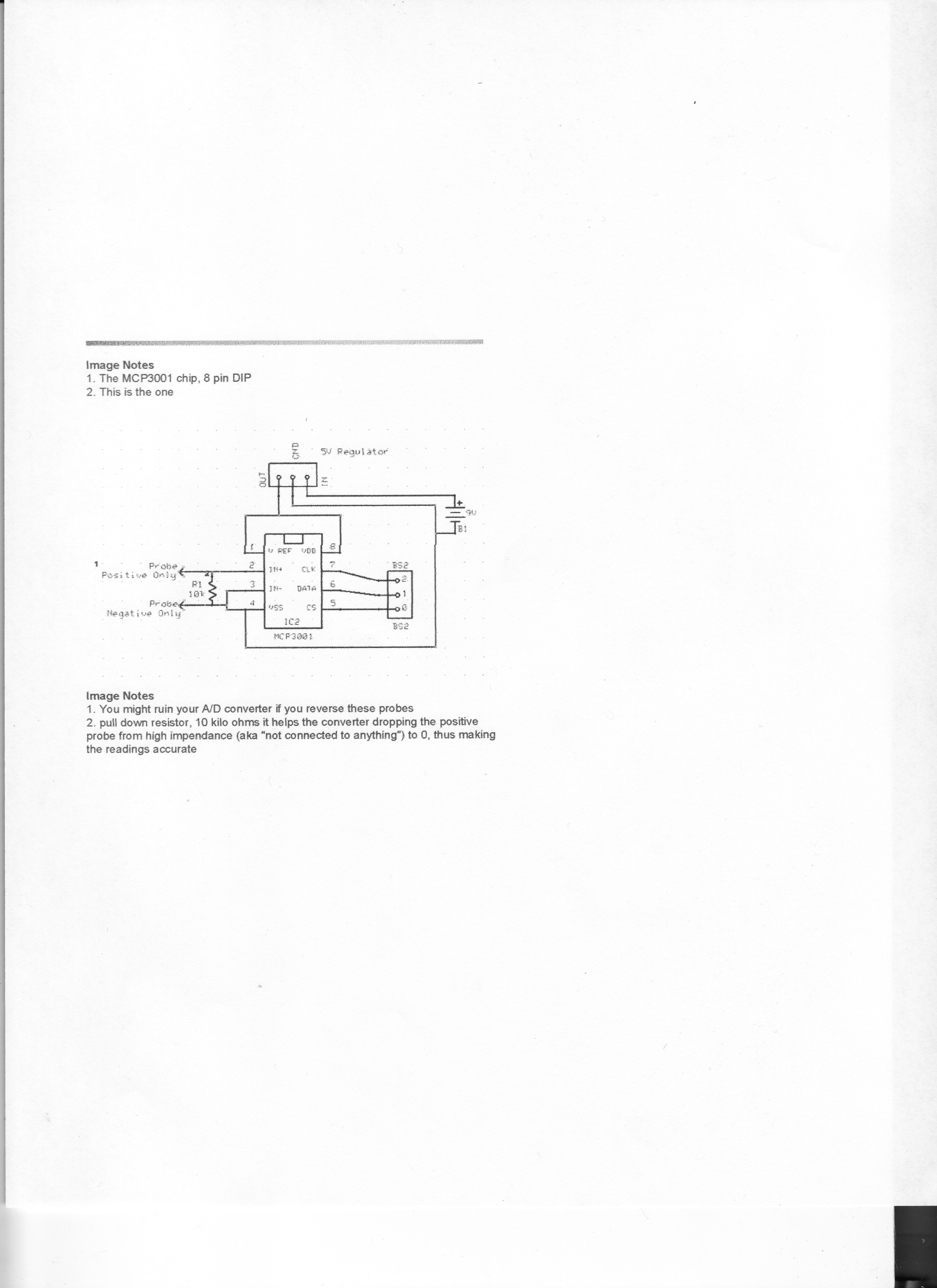
I've tried Using MCP3001 a Microchip 10-bit A/D converter with BS2.· The converter has SPI serial interface, and is 8 pin DIP.· I connected it to my BS2 homework bd. in the manner shown on an attachment to this post.· Is it possible that the MCP3001 cannot be used on a BS2?
·I found this circuitry information on the net at this address:
http://www.instructables.com/id/Digital-Voltmeter/Digital-Voltmeter.pdf· .
According to the MCP3001 data sheet:
http://www.microchip.com/wwwproducts/Devices.aspx?dDocName=en010527· "The MCP3001 features a successive approximation register (SAR) architecture and an industry-standard SPI serial interface, allowing 10-bit ADC capability to be added to any PIC® microcontroller."
I put the circuitry together for DIGITAL VOLTMETER. I used an MCP3001 and connected it to my BS2 microcontroller kit (PIC16C57C), as shown on the diagram of the instruction sheet. I downloaded the Pbasic code and entered it directly into my Basic Stamp editor. To check out the circuitry, I applied a 1.5v battery, the +terminal, to pin 2 of the MCP, (with neg to gnd).· My output was·Zero's for all. So attached a 3v battery in the same manner with the same results: a lot of zero's. I looked over the code, it was exactly the same as·the download, checked the circuitry hook-ups, numerous times; can't find anything out of place. I have the 10k pull down resistor in place, which is MCP pin-2 to gnd.·
In the code is the statement: "make sure there is a pull-up resistor (10k) on the data pin". I did this too, still no help, still getting zero's.
MAIN PART OF CODE:
THANKS,· PO2LE
·I found this circuitry information on the net at this address:
http://www.instructables.com/id/Digital-Voltmeter/Digital-Voltmeter.pdf· .
According to the MCP3001 data sheet:
http://www.microchip.com/wwwproducts/Devices.aspx?dDocName=en010527· "The MCP3001 features a successive approximation register (SAR) architecture and an industry-standard SPI serial interface, allowing 10-bit ADC capability to be added to any PIC® microcontroller."
I put the circuitry together for DIGITAL VOLTMETER. I used an MCP3001 and connected it to my BS2 microcontroller kit (PIC16C57C), as shown on the diagram of the instruction sheet. I downloaded the Pbasic code and entered it directly into my Basic Stamp editor. To check out the circuitry, I applied a 1.5v battery, the +terminal, to pin 2 of the MCP, (with neg to gnd).· My output was·Zero's for all. So attached a 3v battery in the same manner with the same results: a lot of zero's. I looked over the code, it was exactly the same as·the download, checked the circuitry hook-ups, numerous times; can't find anything out of place. I have the 10k pull down resistor in place, which is MCP pin-2 to gnd.·
In the code is the statement: "make sure there is a pull-up resistor (10k) on the data pin". I did this too, still no help, still getting zero's.
MAIN PART OF CODE:
cs PIN 0·············· 'chip select is pin 0
clk PIN 1·············· 'clock is pin 1
dat PIN 2············· 'dat is pin 2
························· ·'make sure there is a pull-up resistor (10k) on the data pin
refv CON 5············ 'reference voltage
refvbin CON 1023··· 'the max value for 10 bits
pt CON 1
value VAR Word····· 'the reading results is stored here
voltage VAR Nib····· 'the calculated voltage is here
HIGH cs··············· 'unselect chip
PAUSE 250
GOTO mainloop:
mainloop:
LOW cs····················· 'select that chip
LOW clk·····················'idle clock cycle 1, two are needed
PAUSE pt
HIGH clk
PAUSE pt
··································· 'idle cycle 2
LOW clk
PAUSE pt
HIGH clk
PAUSE pt
··································· 'end idle clock cycles, start null bit
LOW clk
PAUSE pt
HIGH clk
PAUSE pt
'end null bit
'start shift in
SHIFTIN dat, clk, MSBPOST, [noparse][[/noparse]value\10]······· ·'shift in serial data
····························································· 'dat and clk pin are defined
·······························································'msbpost means read bit after clock cycle
·······························································'the 10 bit data is stored into "value"
······························································ 'change the 10 to the resolution of your chip
HIGH cs························ 'unselect chip
voltage = (value * 100 / 1023) * refv / 100···
DEBUG HOME
DEBUG "Binary Read: "
DEBUG BIN value
DEBUG "············ ", CR
DEBUG "Decimal Read: "
DEBUG DEC value
DEBUG "············ ", CR
DEBUG "Voltage: "
DEBUG DEC voltage, CR·········· 'this is rounded down
DEBUG ? voltage
PAUSE 1····························· 'loop delay
value = 0··························· ·'resets the value variable
voltage = 0··························'resets the voltage variable
GOTO mainloop···················· 'repeat
THANKS,· PO2LE
3397 x 4672 - 2M
Comments
▔▔▔▔▔▔▔▔▔▔▔▔▔▔▔▔▔▔▔▔▔▔▔▔
- Stephen
I used the Pbasic code for operating·an·ADC0831 8-bit analog-to-digital converter
this code·is included with the basic stamp editor's help file.· It worked to a certain extent, but the output was not right.
' 8-bit analog-to-digital converter from National Semiconductor.
Main:
· DO
··· LOW CS····································· ' activate the ADC0831
··· SHIFTIN AData, Clk, MSBPOST, [noparse][[/noparse]adcRes\9]···· ' shift in the data
··· HIGH CS···································· ' deactivate ADC0831
··· DEBUG ? adcRes····························· ' show conversion result
··· PAUSE 1000································· ' wait one second
· LOOP········································· ' repeat
· END
▔▔▔▔▔▔▔▔▔▔▔▔▔▔▔▔▔▔▔▔▔▔▔▔
Chris Savage
Parallax Engineering