

PCB Layout Technique - Good Stuff
 CannibalRobotics
Posts: 535
CannibalRobotics
Posts: 535
I was at a Texas Instruments semenar on PCB layout·yesterday. The presenter said several things that really stuck in my mind so I thought I'd pass them along. Some of it is common sense but other is not.
1) Fill vias,·on a·microscopit level, it's an empty metal can. It forms inductors that projects noise. Filling them with solder helps.
2) Don't split analog and digital ground planes as it leaves only components to straddle the bridge.
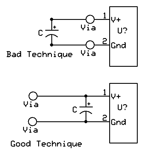
3) Bypass caps should be as close as possible to the component and on the component side of any via. (see the pic below)
4) Regionalize your board as much as possible keeping analog, digital, High frequency, low frequency seperated.
5) Don't use vias on high frequency lines like clocks.
6) If your using a 4 or six layer board, try to sandwich the traces between ground and power plane.
Food for Thought.
Cheers and Happy Halloween.
Jim-
▔▔▔▔▔▔▔▔▔▔▔▔▔▔▔▔▔▔▔▔▔▔▔▔
Signature space for rent, only $1.
Send cash and signature to CannibalRobotics.
1) Fill vias,·on a·microscopit level, it's an empty metal can. It forms inductors that projects noise. Filling them with solder helps.
2) Don't split analog and digital ground planes as it leaves only components to straddle the bridge.
3) Bypass caps should be as close as possible to the component and on the component side of any via. (see the pic below)
4) Regionalize your board as much as possible keeping analog, digital, High frequency, low frequency seperated.
5) Don't use vias on high frequency lines like clocks.
6) If your using a 4 or six layer board, try to sandwich the traces between ground and power plane.
Food for Thought.
Cheers and Happy Halloween.
Jim-
▔▔▔▔▔▔▔▔▔▔▔▔▔▔▔▔▔▔▔▔▔▔▔▔
Signature space for rent, only $1.
Send cash and signature to CannibalRobotics.
Comments
I agree with some of that but dissagree with these:
Filling vias doesn't sound like a good idea. And, it won't affect inductance of high-freq signals at all.
I think there are many cases where a seperate analog ground is a good idea.
For a 4-layer board, I think the middle 2 should be power and ground. <-- I take this one back.· If you have high-freq. signals, it might be wise to sandwich them as suggested.
▔▔▔▔▔▔▔▔▔▔▔▔▔▔▔▔▔▔▔▔▔▔▔▔
Chris Savage
Parallax Engineering