

Question on how to use multiple SHIFTOUT commands or other method with differen
 T&E Engineer
Posts: 1,396
T&E Engineer
Posts: 1,396
I tried researching this on the forum and did not see anything similar to what I am trying to do.
I am trying to control·basically·4 sets of·displays of LEDs that use multiple 74HC595s. What I need to do is something like this:
SHIFTOUT Dpin1, Clk, MSBFIRST, pattern1
SHIFTOUT Dpin2, Clk, MSBFIRST, pattern1
SHIFTOUT Dpin3, Clk, MSBFIRST, pattern1
SHIFTOUT Dpin4, Clk, MSBFIRST, pattern1
Low Strobe
:
:
As you can see there is Dpin1 to·Dpin4 in the·4 SHIFTOUT commands.
When I use a configuration like this I see the LEDs scroll correctly but are off by 8 LEDs between each display - as I would expect because pattern1 is 8 bits.
What I would like to do is·modify SHIFTOUT or some other method to have·all sets of LEDs scroll at the same time (not 8 LEDs off).
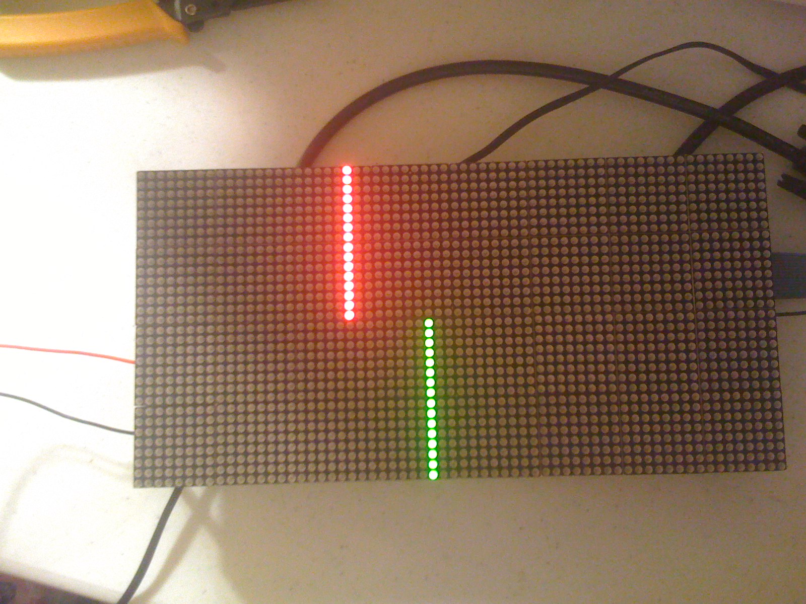
The attached picture indicates what it looks like with 2 SHIFTOUT commands (see program listing in next post).
Something like SHIFTOUT Dpin1,·Dpin2, Dpin3, Dpin4, Clk, MSBFIRST,·pattern1·would be nice but not·possible using the standard SX/B SHIFTOUT command.
I was going to try using 4 different Clk pins for each of the statements but havent tried that yet. Im thinking that won't work because of pattern1 still being 8 bits.
Any ideas how to acheive the same data shifting over·4 Datapins?
Thanks.
Post Edited (T&E Engineer) : 6/14/2008 7:34:20 PM GMT
I am trying to control·basically·4 sets of·displays of LEDs that use multiple 74HC595s. What I need to do is something like this:
SHIFTOUT Dpin1, Clk, MSBFIRST, pattern1
SHIFTOUT Dpin2, Clk, MSBFIRST, pattern1
SHIFTOUT Dpin3, Clk, MSBFIRST, pattern1
SHIFTOUT Dpin4, Clk, MSBFIRST, pattern1
Low Strobe
:
:
As you can see there is Dpin1 to·Dpin4 in the·4 SHIFTOUT commands.
When I use a configuration like this I see the LEDs scroll correctly but are off by 8 LEDs between each display - as I would expect because pattern1 is 8 bits.
What I would like to do is·modify SHIFTOUT or some other method to have·all sets of LEDs scroll at the same time (not 8 LEDs off).
The attached picture indicates what it looks like with 2 SHIFTOUT commands (see program listing in next post).
SUB OUT
  FOR temp1 = 7 to 0 step -1

  SHIFTOUT R1_Dpin, S_Cpin, MSBFIRST, ~pattern(temp1)' send the bits
  SHIFTOUT G2_Dpin, S_Cpin, MSBFIRST, ~pattern(temp1)' send the bits


  NEXT
  PULSOUT L_Latch, 1                               ' transfer to outputs
ENDSUB
Something like SHIFTOUT Dpin1,·Dpin2, Dpin3, Dpin4, Clk, MSBFIRST,·pattern1·would be nice but not·possible using the standard SX/B SHIFTOUT command.
I was going to try using 4 different Clk pins for each of the statements but havent tried that yet. Im thinking that won't work because of pattern1 still being 8 bits.
Any ideas how to acheive the same data shifting over·4 Datapins?
Thanks.
Post Edited (T&E Engineer) : 6/14/2008 7:34:20 PM GMT
1600 x 1200 - 391K
Comments
The picture indicates using the RA output to A, B, C, and D - not the 74LS193 IC and pulse generator test.
By changing the SHIFTOUT command to have either R1_Dpin, R2_Dpin, G1_Dpin or G2_Dpin entered, it will allow either the top 16 rows or bottom 16 rows in either red or green.
If the scanning is fast (within the Interrupt routine), all I see is a straight line from the top row to the bottom 16th row (using R1_Dpin - means the top 16 rows in color RED).
If I change the data going into the SHIFTOUT command (e.g. pattern(temp1)), I can see that but all 16 rows have that same pattern (in this case a straight line).
I know that picture looks like there are 2 columns of 16 rows of LEDs on - it is only 1 as I could not snap the picture fast enough .
' ========================================================================= ' ' File...... 6432a.SXB ' Purpose... Display information on 64x32 BiColor LED display ' Author.... Tim Gilmore ' E-mail.... ' Started... 13 June 2008 ' Updated... ' ' ========================================================================= ' ------------------------------------------------------------------------- ' Program Description ' ------------------------------------------------------------------------- ' ------------------------------------------------------------------------- ' Device Settings ' ------------------------------------------------------------------------- DEVICE SX28, OSC4MHZ, TURBO, STACKX, OPTIONX, BOR22 FREQ 4_000_000 ' ------------------------------------------------------------------------- ' IO Pins ' ------------------------------------------------------------------------- Row PIN RA OUTPUT 'Controls A, B, C, and D on the display board (0-15 rows) S_Cpin VAR RB.0 ' shift clock L_Latch VAR RB.1 ' latch outputs R1_Dpin VAR RB.2 ' shift R1 data 'Red LEDs in top 16 rows R2_Dpin VAR RB.3 ' shift R2 data 'Red LEDs in bottom 16 rows G1_Dpin VAR RB.4 ' shift G1 data 'Green LEDS in top 16 rows G2_Dpin VAR RB.5 ' shift G2 data 'Green LEDS in bottom 16 rows ' ------------------------------------------------------------------------- ' Constants ' ------------------------------------------------------------------------- DelayTime CON 50 'Column speed of scrolling LED display ' ------------------------------------------------------------------------- ' Variables ' ------------------------------------------------------------------------- tmpW1 VAR Word temp1 VAR Byte ' subroutine work vars pattern VAR Byte(8) ' pattern for LEDs idx VAR Byte ' ------------------------------------------------------------------------- INTERRUPT 2500 ' 0.4 ms rate ' ------------------------------------------------------------------------- 'Scans 16 rows of LED Display board - RA. ISR_Start: IF Row < 15 THEN INC Row ' point to next row ELSE Row =0 ' wrap back ENDIF ISR_Exit: RETURNINT ' ========================================================================= PROGRAM Start ' ========================================================================= ' ------------------------------------------------------------------------- ' Subroutine Declarations ' ------------------------------------------------------------------------- DELAY_MS SUB 1, 2 ' delay in milliseconds OUT SUB 0 ' move value to 74HC595 FORWARD SUB 0 ' ------------------------------------------------------------------------- ' Program Code ' ------------------------------------------------------------------------- Start: 'PLP_B = %10000000 ' pull-up unused pins PLP_A = %1111 ' pull-up unused pins PLP_B = %00111111 PLP_C = %00000000 LOW L_Latch ' make an output and low pattern = %00000001 ' initialize pattern Main: FORWARD GOTO Main End ' ------------------------------------------------------------------------- ' Subroutine Code ' ------------------------------------------------------------------------- ' Use: DELAY_MS ms ' -- delay program for 'ms' milliseconds SUB DELAY_MS IF __PARAMCNT = 1 THEN ' byte parameter? tmpW1 = __PARAM1 ELSE tmpW1 = __WPARAM12 ENDIF PAUSE tmpW1 ENDSUB ' ------------------------------------------------------------------------- SUB OUT FOR temp1 = 7 to 0 step -1 SHIFTOUT R1_Dpin, S_Cpin, MSBFIRST, ~pattern(temp1)' send the bits NEXT PULSOUT L_Latch, 1 ' transfer to outputs ENDSUB 'R1_Dpin is used to use Red LEDS in the top 16 rows of the LED Display ' ------------------------------------------------------------------------- 'Routine to scroll columns (64 LEDs) on the LED Display board's multiple 74HC595 ICs. SUB FORWARD idx = 0 pattern(0) = %00000001 DO OUT DELAY_MS DelayTime ' hold pattern(0) = pattern(0) << 1 ' shift pattern left INC idx LOOP UNTIL idx = 8 idx = 0 pattern(1) = %00000001 DO OUT DELAY_MS DelayTime ' hold pattern(1) = pattern(1) << 1 ' shift pattern left INC idx LOOP UNTIL idx = 8 idx = 0 pattern(2) = %00000001 DO OUT DELAY_MS DelayTime ' hold pattern(2) = pattern(2) << 1 ' shift pattern left INC idx LOOP UNTIL idx = 8 idx = 0 pattern(3) = %00000001 DO OUT DELAY_MS DelayTime ' hold pattern(3) = pattern(3) << 1 ' shift pattern left INC idx LOOP UNTIL idx = 8 idx = 0 pattern(4) = %00000001 DO OUT DELAY_MS DelayTime ' hold pattern(4) = pattern(4) << 1 ' shift pattern left INC idx LOOP UNTIL idx = 8 idx = 0 pattern(5) = %00000001 DO OUT DELAY_MS DelayTime ' hold pattern(5) = pattern(5) << 1 ' shift pattern left INC idx LOOP UNTIL idx = 8 idx = 0 pattern(6) = %00000001 DO OUT DELAY_MS DelayTime ' hold pattern(6) = pattern(6) << 1 ' shift pattern left INC idx LOOP UNTIL idx = 8 idx = 0 pattern(7) = %00000001 DO OUT DELAY_MS DelayTime ' hold pattern(7) = pattern(7) << 1 ' shift pattern left INC idx LOOP UNTIL idx = 8 ENDSUBThe·6432 Bicolor LED display and manual (too big to attach) can be found here:
·http://www.sureelectronics.net/goods.php?id=147
Post Edited (T&E Engineer) : 6/14/2008 7:27:55 PM GMT
' MSBFIRST

chopomatic:

  bitmask = %1000 0000

  FOR hotdog = 1 TO 8

    B_beef = beef & bitmask
    B_beef = B_beef / 128         'same as >> 7; will be RB bit0
    B_pork = pork & bitmask
    B_pork = B_pork / 64          'same as >> 6; will be RB bit1
    B_chicken = chicken & bitmask
    B_chicken = B_chicken / 32    'same as >> 5; will be RB bit2
    B_turkey = turkey & bitmask
    B_turkey = B_turkey / 16      'same as >> 4; will be RB bit3

    RB = B_beef + B_pork + B_chicken + B_turkey

    Pulsout CLKpin
    [s]bitmask = bitmask * 2[/s]

    beef = beef << 1
    pork = pork << 1
    chicken = chicken << 1
    turkey = turkey << 1

    NEXT hotdog
Post Edited (PJ Allen) : 6/15/2008 5:03:05 PM GMT
So if I understand you correctly....using·my original reference below:
I'm not sure if I understand completely but here is my rendition if correct?
Post Edited (T&E Engineer) : 6/15/2008 5:55:19 PM GMT
I think I have 2 issues (at least for now):
1. Be able to use multiple SHIFTOUT statements to control RED and GREEN LEDs in both upper and lower 16 row sections (e.g. R1, R2, G1, G2). I think I may be able to do this in hardware but still pondering this at the moment.
2. The second issue deals more with the Row scanning. If I was to enter in ROW = 1 (e.g. RA = 1) the display doesn't turn the LEDs on. I would think this would turn on Row 1 so that what ever data is shifted out·of the 74HC595s (controlled by SHIFTOUT statements) would be displayed. If I use something like this:
Row····· PIN·RA·· OUTPUT·· 'Controls A, B, C, and D on the display board (0-15 rows) which goes to 74HC138 3-8 decoders on the board.
·IF Row < 15 THEN
··· INC Row·····' point to next row
· ELSE
··· Row =0·····' wrap back
· ENDIF
It turns on a solid stream of LEDs from Row 0 to 15 (up to down). I wanted to be able to control this with individual row access with something like Row =·3 or RA = %0011 to only turn on the SHIFTOUT column data on row 3.
I hope this is a little more clear for those who are following.
I have yet to get an example code from the manufacturer in China - although it was promised with no response yet.
Thanks again!
Here, figuring that they are Bytes, I am routing R1 through RB.0, R2 through RB.1, G1 through RB.2, G2 through RB.3.· Once a bit from each has been put on the RB bus, a PULSOUT is·done on RB.7.·
TRIS_B = $00

R1         var  byte
R2         var  byte
G1         var  byte
G2         var  byte
b_R1       var  byte
b_R2       var  byte
b_G1       var  byte
b_G2       var  byte
bitmask    var  byte
hotdog     var  byte

PROGRAM Start

Start:

RB = 00

chopomatic:

  bitmask = $80

  FOR hotdog = 1 TO 8

    B_R1 = R1 & bitmask           ' 0 or bitmask
    B_R1 = B_R1 / bitmask         ' 0 or 1
    RB.0 = B_R1
    B_R2 = R2 & bitmask           ' 0 or bitmask
    B_R2 = B_R2 / bitmask         ' 0 or 1
    RB.1 = B_R2
    B_G1 = G1 & bitmask     ' 0 or bitmask
    B_G1 = B_G1 / bitmask   ' 0 or 1
    RB.2 = B_G1
    B_G2 = G2 & bitmask       ' 0 or bitmask
    B_G2 = B_G2 / bitmask     ' 0 or 1
    RB.3 = B_G2

   ' the RB bits have been set, ready to pulse clock for external latch

    Pulsout RB.7, 2

    bitmask = bitmask / 2     ' 1_$40, 2_$20, 3_$10, 4_$08, 5_$04, 6_$02, 7_$01, 8_XX

    NEXT hotdog
  END
Post Edit -- That's SHIFTOUT'ing on multiple pins, MSBFIRST, which·is what I·thought you were asking for.
In my previous example, I thought that I was preserving the pattern data, but I was manipulating it.· In this example, I am not; I am changing the maskbit each time through.
-- 6/20/08
-- 6/21/08
Post Edited (PJ Allen) : 6/21/2008 1:08:31 PM GMT
I so very much appreciate you spending time to help me.
Have you had a chance to download the manual for the 6432 Dot Matrix BiColor Display Information Board that this coding is being written for? Here is the link: http://www.sureelectronics.net/goods.php?id=147·and more specifically http://www.sureelectronics.net/pdfs/DE-DP030_Ver1.0_EN.pdf·for the manual. You will see in the begining of Chapter 3 a port definition table:
Inconsistencies I found were there was no GND pin, ST is actually labeled as L on the pin header and CK is labeled as S on the pin header. Power to the board is through a +5VDC and GND connector on the back of the board which I am using a 5VDC 20A power supply for this board. I am also running a ground wire from this to my professional development board which has my SX-28 and cable from the Display Board.
Normally with a 74HC595 and a SHIFTOUT statement, I would use ST (or L for Latching), CK (or S for Clock) and (R1, R2, G1 or G2) for the Data pin. This may be a bit clearer in my original full program listing (see post #2).
Also I am using pins A, B, C and D (for Row scanning) to go to the SX-28's RA for a 0-15 counter - to the Display Boards 74HC138.
I am showing this to you because R1, R2, G1 and G2 are actually Data "pins" and not VAR "Bytes" as described in your program. Perhaps this is what also is hanging me up with understanding how this all·ties together.
Thank you again for your understanding.
PJ in his usual cleverness *is* treating those 4 pins as clocked (shiftout) data -- what his routine does is put each bit from each of 4 patterns onto all 4 data pins simultaneously, then clocks it. Essentially he "bit banged" 4 simultaneous shiftout routines.
On the first loop through, the first bit of each of the 4 pattern bytes is put on that pattern's respective data pin. Then a clock pulse is generated. Then the next bit for each of the 4 patterns is put on each of the 4 data pins. Then a clock pulse. Repeat. It doesn't look like his code shows pulsing the latch, just sending the data (but that should be easy enough for you to insert).
My only comment on PJ's code would be to replace the divides with shift rights ( >> ) -- will save huge amounts of codespace on the SX. Or, at the least, I would wrap the divide into a function (a divide takes a lot of code space).
I would run your ABCD scans separately in an ISR (interrupt) unless there is reason to do otherwise. This would also let you adjust the scan rate *independently* of how fast you are clocking out new pixel data, etc.
▔▔▔▔▔▔▔▔▔▔▔▔▔▔▔▔▔▔▔▔▔▔▔▔
When the going gets weird, the weird turn pro. -- HST
1uffakind.com/robots/povBitMapBuilder.php
1uffakind.com/robots/resistorLadder.php
So according to PJ's program, I can coordinate the data pins as follows:
Display Board Port pin "R1" is connected to SX-28 pin·RB.0
Display Board Port pin "R2" is connected to SX-28 pin RB.1
Display Board Port pin "G1" is connected to SX-28 pin RB.2
Display Board Port pin "G2" is connected to SX-28 pin RB.3
Display Board Port pin "CK" (Clock) is connected directly to SX-28 pin RB.7
Finally
Display Board Port pin "A" is connected directly to SX-28 pin RA.0
Display Board Port pin "B" is connected directly to SX-28 pin RA.1
Display Board Port pin "C" is connected directly to SX-28 pin RA.2
Display Board Port pin "D" is connected directly to SX-28 pin RA.3
Display Board Port pin "EN" (Enable) is connected directly to ground
Display Board Port pin "ST" (Latch) is connected directly (to SX-28 pin RB.5 or RB.6)
Add a statement like PULSEOUT RB.5, 2 after the FOR NEXT "hotdog" loop.
If this is correct, I will try this tomorrow night after work.
Thanks!
Actually, looking over the spec sheet and PJ's code again, there is no reason you couldn't lay it out this way:
RC -- scan ABCD (4)
RB -- G1G2R1R2 data lines (4)
RA -- shared latch and clock pins (2)
This way you could add another board (!) without recoding much or rewiring (ABCD-01/ABCD-02 on RC, G1G2R1R2-01/G1G2R1R2-02 on RB). And that still leaves two pins on RA if you need Tx/Rx to another device.
▔▔▔▔▔▔▔▔▔▔▔▔▔▔▔▔▔▔▔▔▔▔▔▔
When the going gets weird, the weird turn pro. -- HST
1uffakind.com/robots/povBitMapBuilder.php
1uffakind.com/robots/resistorLadder.php
I will look it over tonight and let you all know my results.
Thanks again to PJ Allen and Zoot!
More specifically was the OUT subroutine which replaces the SHIFTOUT routine.
It clearly shows the R1, R2, G1 and G2 datapins as well as Clock and Latch. However before it used pattern(temp1) to indicate the actual data being shifted. Using this new format, it is unclear how this is to be laid out. I am guessing something like: pattern(temp1) = RB but really not sure.
SUB OUT

  bitmask = $80

  FOR temp1 = 7 to 0 step -1

  FOR hotdog = 1 to 8

    B_R1 = R1 & bitmask           ' 0 or bitmask
    B_R1 = B_R1 / bitmask         ' 0 or 1
    R1_Dpin = B_R1
    B_R2 = R2 & bitmask           ' 0 or bitmask
    B_R2 = B_R2 / bitmask         ' 0 or 1
    R2_Dpin = B_R2
    B_G1 = G1 & bitmask           ' 0 or bitmask
    B_G1 = B_G1 / bitmask         ' 0 or 1
    G1_Dpin = B_G1
    B_G2 = G2 & bitmask           ' 0 or bitmask
    B_G2 = B_G2 / bitmask         ' 0 or 1
    G2_Dpin = B_G2

   ' the RB bits have been set, ready to pulse clock for external latch

    Pulsout S_Cpin, 2

    bitmask = bitmask / 2     ' 1_$40, 2_$20, 3_$10, 4_$08, 5_$04, 6_$02, 7_$01, 8_XX

  NEXT

  [b]pattern(temp1) = RB[/b]

  NEXT

  PULSOUT L_Latch, 2                               ' transfer to outputs

ENDSUB
You will see the FORWARD routine calls out the OUT subroutine which used before
SHIFTOUT R1_Dpin, S_Clk, MSBFIRST, pattern(temp1)
So where·does pattern(temp1) fit into this new routine?
Thanks!
On a side note, I had a couple of P channel FETs blow out on the display board. I'm wondering if the manufacturer uses the same FET for both Red and Green LEDs. The manual/datasheet never states using both on at the same time to get a yellowish/orange LED effect. I tried to turn both LEDs on at the same time during some trial coding and saw the smoke and smelled the burn. A bit surprising but I beleive I can repair it when the parts arrive. In the mean time, I just have to acknowledge that both upper and lower Rows 12, 2 and 4 are out on the LED display temporarily.
Bean.
▔▔▔▔▔▔▔▔▔▔▔▔▔▔▔▔▔▔▔▔▔▔▔▔
- - - - - - - - - - - - - - - - - - - - - - - - - - - - - - -
Uhhhm, that was on fire when I got here...
www.iElectronicDesigns.com
Post Edited (Bean (Hitt Consulting)) : 6/22/2008 1:51:06 AM GMT
Now I know·(if I can just·remember.)
Still, my colleague and I are stumped why plugging a value into RA (given TRIS_A = $00) isn't setting the display line, but that that does happen with the INTERRUPT method he has from another program.· (I'd like to see that with a 'scope.)
Post Edited (PJ Allen) : 6/22/2008 2:05:36 AM GMT
Row PIN RA·· OUTPUT
'
· INTERRUPT 2500··· ' 0.4 ms rate
'
ISR_Start:
· IF Row < 15 THEN
··· INC Row···· ' point to next row
· ELSE
··· Row =0···· ' wrap back
· ENDIF
ISR_Exit:
· RETURNINT
If the row counter (or even simply just an "INC Row" or INC RA) is running, I see the LEDs turn on. This is a row/line scanning routine.
But if I comment out the Interrupt routine, and just use a INC Row or INC RA from within the Main: program, no LEDs turn on.
This makes no sense to me. Can someone shed some light to this? See the Chopomatic_pt.sxb program from my past post with the pictures.
It has stump both PJ Allen and myself to this. We are ready to use an Oscope Monday if needed but hope we don't have to.
THanks!
Bean.
▔▔▔▔▔▔▔▔▔▔▔▔▔▔▔▔▔▔▔▔▔▔▔▔
- - - - - - - - - - - - - - - - - - - - - - - - - - - - - - -
Uhhhm, that was on fire when I got here...
www.iElectronicDesigns.com
·
This routine turns on all 16 lines/rows (up/down) as it goes across (right to left) each of the 64 columns 1 by 1.
I would think I could simply get rid of the Interrupt routine and just use something like an INC RA in the Main: loop but no LEDs every light up if the Interrupt (same) is commented.
Thanks again for your help Bean!
I would try putting the "INC Row" in the Delay_MS routine by making a loop instead of one big pause.
Something like:
SUB DELAY_MS
· IF __PARAMCNT = 1 THEN ' byte parameter?
··· tmpW1 = __PARAM1
· ELSE
··· tmpW1 = __WPARAM12
· ENDIF
· DO
··· PAUSE 1
··· INC Row ' Since Row is RA there are only 4 bits anyway, so no need to limit the value
··· DEC tmpW1
··LOOP UNTIL tmpW1 = 0
ENDSUB
Bean.
▔▔▔▔▔▔▔▔▔▔▔▔▔▔▔▔▔▔▔▔▔▔▔▔
- - - - - - - - - - - - - - - - - - - - - - - - - - - - - - -
Uhhhm, that was on fire when I got here...
www.iElectronicDesigns.com
·
I have attached an updated version of your suggestion and that does indeed work with the INTERUPT 2500 line commented out using the sugestion inside of the DELAY_MS routine to INC Row.
This is fine for incrementing row (as it looks like a solid line up and down). Is there anyway to ONLY turn on lets say line / row 5 ? or maybe lines/rows· 5 - 10 ?
(e.g. even using LOW Row or HIGH Row (within the DELAY_MS routine with the INC Row commented out displays nothing)) - Only INC Row turns the LEDs on (whether in the interrupt or in the DELAY_MS routine).???
I'm also concerned that eventually sending out character data will have to be in an array. As a Beta tester, the new version of SX/B (un-released) will allow for arrays larger than 16 which will help - but in a display that has 64 columns and 2 sets of 16 rows/lines (in both RED and GREEN LEDs) - Is it pratical to use an array on an SX-28?
Thanks for the great work and I'm awaiting your response.
Post Edited (T&E Engineer) : 6/22/2008 3:23:31 PM GMT
As a test I wired up (2) 74HC138s and cascaded them for 16·LED outputs (too bad the Professional Development Board LEDs want to see +5v - had to wire up 16 negative input LEDs/resistors).
I hardwired the A B C D inputs from the cascaded 74HC138's into either +5vdc or GND and saw the appropriate individual LED turn on as it should. I then took RA from the SX-28 and disconnected it from the LED Display board and connected it to the inputs on the cascaded 74HC138s. I·WAS able to··not have to use INC Row in the routine below (from previous 6232c.sxb attachment)·- but·INSTEAD I could use Row = 8 and I saw LED 8 turn on.
The coding below shows Row = 8 commented out (and INC Row not commented) which is how it works on the LED Display Board.
SUB DELAY_MS
  IF __PARAMCNT = 1 THEN ' byte parameter?
    tmpW1 = __PARAM1
  ELSE
    tmpW1 = __WPARAM12
  ENDIF
  DO
    PAUSE 1

    [b]INC Row[/b] ' Since Row is RA there are only 4 bits anyway, so no need to limit the value  (This works identical to Interrupt routine)

    '[b]Row = 8[/b]   '--> Can't set Row to a single value on this LED display board (does work on 2 cascaded 74HC138s with 16 LEDs) ???

    DEC tmpW1
  LOOP UNTIL tmpW1 = 0
  ENDSUB
This tells me that SX/B can use a statement like Row = 8 (as I have also seen in·other SX/B example coding)
This leads me to believe that the A B C D inputs on the Display board (although going through a buffer first before the 74HC138 - as shown in the manual/datasheet schematics), doesn't work as I would think. What we know is that the INC Row command works on this board but the Row = 8 (or some other # between 0 and 15) does not.
Since I had blown some FETs on this display board earlier (messing with the code), I thought perhaps a buffer or 74HC138 got damaged or something (which I almost didn't buy because the INC Row did work on this LED Display board).
I had boughten a second LED Display board that had never been powered up. I wired in power and the cable to the SX-28 on the Professional Developement Board (PDB) and the code using the INC Row worked as it did on the other board but the Row = 8 did not work (as it did not work on the other board).
This tells me that both LED Display boards are working (with the exception of some burnt out FETs on my "developing" current board. I moved back to the "developing" LED Display board and wired it back up to continue this investigation.
HERE IS THE QUESTION:
I don't know why these boards (which use buffers and cascaded 74HC138s) can not see a Row = xx but an INC Row works. However, using 2 standard cascaded 74HC138's both Row = xx and INC Row does work as it should.
I have gotten no help from the manufacturer on this either (in China) - http://www.sureelectronics.net/goods.php?id=147
6432 Manual/datasheet: http://www.sureelectronics.net/pdfs/DE-DP030_Ver1.0_EN.pdf
Similar board (6416) this was developed from (a bit more information in the datasheet): http://www.sureelectronics.net/goods.php?id=146
6416 Manual/Datasheet (similar board): http://www.sureelectronics.net/pdfs/DE-DP029_Ver1.0_EN.pdf
Comments?????
Something is not quite right about the LED Display board (in that the schematic could also use some better detail too).
More to report on tonight or tomorrow morning.
1. I was able to replace a burnt out MOSFET so Row/Line 12 (upper and lower displays) now lights up.
2. But the better news is that that manufacture "Finally" wrote back and answered some questions about the display board and provided some demonstration code (from what it looks like).
I don't program in "C" but I can probably figure it out to get something in SX/B like it. Although from briefly looking it over, it doesn't look like it does too much.
From Sure Electronics:
16··pieces of APM4953s, Dual channel P-FETs, are controlled by decoders( 2 pieces of 74HC138s) to enable each line (16 lines in all).
Now that the type of microchip we are using is PIC18F4520, on basis of which I have wroten some code in C language. That may be helpful to you. As there are some detailed notes in my code.
Code as follows:
/*This program is used to illuminate  the  first  line  of  6432,every other 5 LEDs*/
/* Encode the Line_SELA, Line_SELB, Line_SELC and Line_SELD differently .That may lead to a line enableded accordingly */
#include<p18f4520.h>

#pragma config OSC = HS             //configure the oscillator 12MHZ
#pragma config PWRT = OFF     // disable Power-up Timer
#pragma config BOREN = OFF   // disable Brown-out Reset
#pragma config WDT = OFF     //disable Watchdog Timer
#pragma config MCLRE = ON    //enable MCLR Pin
#pragma config PBADEN = OFF  //disable PORTB A/D
#pragma config LVP = OFF       //disable Single-Supply ICSP

#define Line_SELA       PORTDbits.RD0
#define Line_SELB       PORTDbits.RD1
#define Line_SELC       PORTDbits.RD2
#define Line_SELD       PORTDbits.RD3

#define Line_EN         PORTEbits.RE2

#define CLK             PORTCbits.RC3
#define LAT             PORTEbits.RE1

#define DAT_R1          PORTDbits.RD4
#define DAT_R2          PORTDbits.RD5
#define DAT_G1          PORTDbits.RD6
#define DAT_G2          PORTDbits.RD7

void init(void)
{
        CMCON=0b00000111;                //Close Comparator
        TRISA=0b00010000;
        TRISB=0b00001111;
        TRISC=0b00000000;                //RC3,RC2output
        TRISD=0b00000000;                //RD0,RD1,RD2,RD3,RD4output
        TRISE=0b00001000;                //RE1,RE2output
        ADCON1=0b00001111;               //Configure Digital Channle
}

void delay_1ms(unsigned char delaytime)
{        unsigned char i, j, k;
        for(i = 0; i < delaytime; i++)
        {
                for(j = 0; j < 200; j++)
                        k--;}
}
void sendone(void)
{
  unsigned char i,k,value;
   Line_EN=0;            //disable to display
   Line_SELA=0;         //select line
   Line_SELB=0;
   Line_SELC=0;
   Line_SELD=0;
for(k=0;k<8;k++)
  {
   value=0xf0;
   for(i=0;i<8;i++)
  {
   DAT_R1=value1 & 0x01;    //choose to illuminate the upper in red
  // DAT_G1=value1 & 0x01;   //choose to illuminate the upper in green
  // DAT_R2= value1 & 0x01;   //choose to illuminate the lower in red
  // DAT_G2= value1 & 0x01;   //choose to illuminate the lower in green
    CLK=0;
    CLK=1;
    value1=value1>>1;
   }
  }

   LAT=0;
   LAT=1;

   Line_EN=1;              //enable to display
   delay_1ms(1);
}

void main(void)
{
init();
// DAT_R1=1;      //choose to turn off  the upper red LEDs
  DAT_R2=1;       // choose to turn off  the  lowr red LEDs
  DAT_G1=1;      // choose to turn off  the  upper green  LEDs
  DAT_G2=1;      // choose to turn off the  lower green  LEDs
while(1)
  {
    sendone();
  }
}
Comments??
What is wrong with this? I get an error INVALID PARAMETER "value1". Is it because DAT_R1 is a bit?
Here is the complete SX/B program:
' ========================================================================= ' ' File...... 6432d.SXB ' Purpose... Display information on 64x32 BiColor LED display ' Author.... Tim Gilmore ' E-mail.... ' Started... 24 June 2008 ' Updated... ' ' ========================================================================= ' ------------------------------------------------------------------------- ' Program Description ' ------------------------------------------------------------------------- ' ------------------------------------------------------------------------- ' Device Settings ' ------------------------------------------------------------------------- DEVICE SX28, OSC4MHZ, TURBO, STACKX, OPTIONX, BOR22 FREQ 4_000_000 ' ------------------------------------------------------------------------- ' IO Pins ' ------------------------------------------------------------------------- Line_SELA VAR RA.0 Line_SELB VAR RA.1 Line_SELC VAR RA.2 Line_SELD VAR RA.3 Line_EN VAR RB.6 CLK VAR RB.0 ' shift clock LAT VAR RB.1 ' latch outputs DAT_R1 VAR RB.2 ' shift R1 data DAT_R2 VAR RB.3 ' shift R2 data DAT_G1 VAR RB.4 ' shift G1 data DAT_G2 VAR RB.5 ' shift G2 data ' ------------------------------------------------------------------------- ' Constants ' ------------------------------------------------------------------------- ' ------------------------------------------------------------------------- ' Variables ' ------------------------------------------------------------------------- tmpW1 VAR Word k VAR Byte value1 VAR Byte i VAR Byte ' ========================================================================= PROGRAM Start ' ========================================================================= ' ------------------------------------------------------------------------- ' Subroutine Declarations ' ------------------------------------------------------------------------- DELAY_MS SUB 1, 2 ' delay in milliseconds INIT SUB 0 SENDONE SUB 0 ' ------------------------------------------------------------------------- ' Program Code ' ------------------------------------------------------------------------- Start: Main: INIT 'DAT_R1 = 1 DAT_R2 = 1 DAT_G1 = 1 DAT_G2 = 1 DO SENDONE LOOP GOTO Main ' ------------------------------------------------------------------------- ' Subroutine Code ' ------------------------------------------------------------------------- SUB INIT TRIS_A = %0000 ' make RA pins outputs TRIS_B = %00000000 ' make RB pins outputs PLP_C = %00000000 ENDSUB ' Use: DELAY_MS ms ' -- delay program for 'ms' milliseconds SUB DELAY_MS IF __PARAMCNT = 1 THEN ' byte parameter? tmpW1 = __PARAM1 ELSE tmpW1 = __WPARAM12 ENDIF PAUSE tmpW1 ENDSUB SUB SENDONE Line_EN = 0 Line_SELA = 0 Line_SELB = 0 Line_SELC = 0 Line_SELD = 0 FOR k = 0 TO 7 value1 = $F0 FOR i = 0 TO 7 DAT_R1 = value1 & $01 'DAT_G1 = value1 & $01 'DAT_R2 = value1 & $01 'DAT_G2 = value1 & $01 CLK = 0 CLK = 1 value1 = value1 >> 1 NEXT NEXT LAT = 0 LAT = 1 Line_EN = 1 DELAY_MS 1 ENDSUB1. value is given a value of $f0 (or 0xf0 in·the "C"·program). However, the rest of the program refers to value as value1. Hopefully, all that is needed is to change value to value1. Can·anyone confirm this?
2. Many of the lines are commented out that maybe should not be for the program to run. What should be and should not be commented out?
3. DAT_R1=value1 & 0x01 in·the "C"·program converts to DAT_R1 = value1 & $01 in my SX/B program. I don't know "C" programming but can figure out that DAT_R1 is a bit from a pin and value1 is a byte so SX/B see's this as an error. Can·anyone confirm if this is how it is supposed to be written?
As a test I changed
DAT_R1··· VAR·RB.2···' shift R1 data
to -> DAT_R1··· VAR·RC···' shift R1 data
And it compiled with no errors in SX/B - but this is not how it should be. It should be a Port pin bit.
How can a Bit from a port pin be equal to a byte as in the "C" program written for a PIC18F4520?
Thanks - standing by!
Post Edited (T&E Engineer) : 6/25/2008 11:38:36 AM GMT
PIC "C" program lines:
#define DAT_R1 · · · ···PORTDbits.RD4
DAT_R1=value1 & 0x01
The PIC simply takes the LSB of value1 and sends it to the DAT_R1 (which is PORTDbits.RD4).
SO...in SX/B this can be simplified to:
DAT_R1 = value.1
Since it also masks off the byte to the LSB anyway.
SX/B compiles now with no errors. I will try this out tonight.
Does this make sense to an PIC "C" programmers?
In the somewhat working SX/B conversion program below there are these 4 lines:
Line_SELA·VAR·RA.0
Line_SELB·VAR·RA.1
Line_SELC·VAR·RA.2
Line_SELD·VAR·RA.3
:
:
Line_SELA = 0
Line_SELB = 1
Line_SELC = 1
Line_SELD = 1
This should turn on Line or Row 7 (from 0 to 15) on the Display. However, it did nothing unless I added something like INC RA in that routine (but then All 16 lines/rows turn on). What I did is added these 4 lines at the bottom of the routine and IT WORKED to all me to control individual Lines/rows.
Line_SELA = ~Line_SELA
Line_SELB = ~Line_SELB
Line_SELC = ~Line_SELC
Line_SELD = ~Line_SELD
Now Line/row 7 displayed the value1 = $F0 data.
This looked ok until I changed value1 data to something else and the data is not quite correct. So something is not right. And still the data in value1 copies its value across the 64 columns of LEDs (8 times).
So using value1 = $F0 displays
ooo----oooo----oooo----oooo----oooo----oooo----oooo----oooo----o
Using value1 = $00 displays
oooooooooooooooooooooooooooooooooooooooooooooooooooooooooooooooo
Using value1 = $FF displays
o
o
o
o
o
o
o
o
o
Using value1 = $AA displays
-o-o-o-o-o-o-o-o-o-o-o-o-o-o-o-o-o-o-o-o-o-o-o-o-o-o-o-o-o-o-o-o
Using value1 = $0F displays
---ooooo---ooooo---ooooo---ooooo---ooooo---ooooo---ooooo---ooooo
As you can see these values are not right.
Here is the program below:
' =========================================================================
'
'   File...... 6432d.SXB
'   Purpose... Display information on 64x32 BiColor LED display
'   Author.... Tim Gilmore
'   E-mail....
'   Started... 24 June 2008
'   Updated...
'
' =========================================================================

' -------------------------------------------------------------------------
' Program Description
' -------------------------------------------------------------------------

' -------------------------------------------------------------------------
' Device Settings
' -------------------------------------------------------------------------
DEVICE          SX28, OSC4MHZ, TURBO, STACKX, OPTIONX, BOR22
FREQ            4_000_000

' -------------------------------------------------------------------------
' IO Pins
' -------------------------------------------------------------------------
Line_SELA VAR RA.0
Line_SELB VAR RA.1
Line_SELC VAR RA.2
Line_SELD VAR RA.3

CLK  VAR RB.0   ' shift clock
LAT  VAR RB.1   ' latch outputs

DAT_R1  VAR RB.2   ' shift R1 data
DAT_R2  VAR RB.3   ' shift R2 data
DAT_G1  VAR RB.4   ' shift G1 data
DAT_G2  VAR RB.5   ' shift G2 data

Line_EN VAR RB.6
' -------------------------------------------------------------------------
' Constants
' -------------------------------------------------------------------------

' -------------------------------------------------------------------------
' Variables
' -------------------------------------------------------------------------
tmpW1  VAR Word

k      VAR Byte

value1 VAR Byte

i      VAR Byte

' =========================================================================
  PROGRAM Start
' =========================================================================

' -------------------------------------------------------------------------
' Subroutine Declarations
' -------------------------------------------------------------------------
DELAY_MS SUB 1, 2   ' delay in milliseconds
INIT     SUB 0
SENDONE  SUB 0

' -------------------------------------------------------------------------
' Program Code
' -------------------------------------------------------------------------
Start:

Main:

INIT

DAT_R1 = 1 'Choose to turn off upper Red LEDs
DAT_R2 = 1 'Choose to turn off lower Red LEDs


'DAT_G1 = 1 'Choose to turn off upper Green LEDs (if commented then - LEDs on)


DAT_G2 = 1 'Choose to turn off lower Green LEDs

DO

SENDONE

LOOP

'GOTO Main

' -------------------------------------------------------------------------
' Subroutine Code
' -------------------------------------------------------------------------
SUB INIT
  TRIS_A = %0000                             ' make RA pins outputs
  TRIS_B = %00000000                            ' make RB pins outputs
  ENDSUB

' Use: DELAY_MS ms
' -- delay program for 'ms' milliseconds
SUB DELAY_MS
  IF __PARAMCNT = 1 THEN   ' byte parameter?
    tmpW1 = __PARAM1
  ELSE
    tmpW1 = __WPARAM12
  ENDIF
  PAUSE tmpW1
  ENDSUB

SUB SENDONE
  Line_EN = 0   'Disable to not display

  Line_SELA = 1  'Turn on Line/row 7 (0-15)
  Line_SELB = 1
  Line_SELC = 1
  Line_SELD = 0

  FOR k = 0 TO 7

  value1 = $0F

  FOR i = 0 TO 7

  'DAT_R1 = value1.1 'Choose to illuminate the upper in red


  DAT_G1 = value1.1  'Choose to illuminate the upper in green


  'DAT_R2 = value1.1 'Choose to illuminate the lower in red
  'DAT_G2 = value1.1 'Choose to illuminate the lower in green

  CLK = 0
  CLK = 1

  value1 = value1 >> 1
  NEXT
  NEXT


'Required statements to control individule Lines/rows
'(or just use INC RA for all 16 Lines/rows on)

  Line_SELA = ~Line_SELA
  Line_SELB = ~Line_SELB
  Line_SELC = ~Line_SELC
  Line_SELD = ~Line_SELD

 'INC RA

  LAT = 0
  LAT = 1

  Line_EN = 1   'Enable to display
  DELAY_MS 1
  ENDSUB
·
Where you have: