

HDMI 4-Channel Oscilloscope Demo
 cgracey
Posts: 14,280
cgracey
Posts: 14,280
in Propeller 2
I was really wanting to see how the scope modes would work to build a simple oscilloscope with trigger. The SCOPE smart pin modes put out 8-bit samples on every clock and perform triggering functions based on signal levels.
So, this little scope program uses the DDS/Goertzel circuit to generate simultaneous sine, triangle, sawtooth, and square wave patterns in an FM mode, so that the frequency wanders between 350KHz and 1MHz. These four DDS output pins can be wired to the scope inputs for stimulus by connecting the following pins together:
P48 and P52
P49 and P53
P50 and P54
P51 and P55
That will give the scope something to trigger off of and display. The scope inputs are:
P52 = channel 0, level-triggers for scope operation
P53 = channel 1
P54 = channel 2
P55 = channel 3
You must drive some signal into channel 0 to generate a trigger, in case you don't use the DDS outputs.
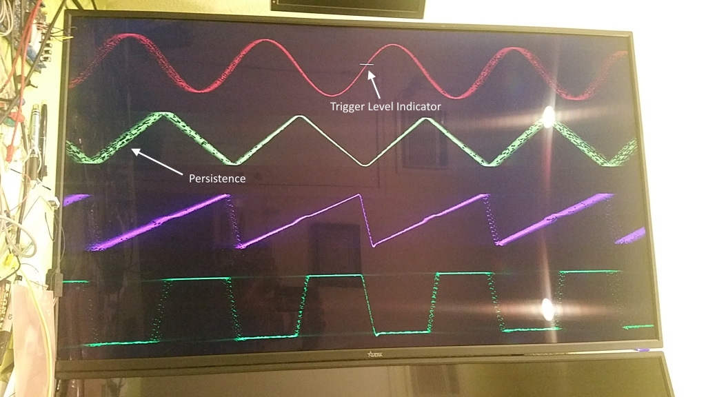
An HDMI monitor connects on P32..P39.
This scope shows four channel traces, sampled every 4th clock in parallel. They could be sampled on every clock, but not much changes in so short of a time. The traces have persistence, so old traces gently fade away as new ones are plotted. It's doing 120 triggers/plots per second, though the monitor refreshes at only 60Hz.
There is an MP4 at the end of this post.
Here is the code. It's 172 longs:
So, this little scope program uses the DDS/Goertzel circuit to generate simultaneous sine, triangle, sawtooth, and square wave patterns in an FM mode, so that the frequency wanders between 350KHz and 1MHz. These four DDS output pins can be wired to the scope inputs for stimulus by connecting the following pins together:
P48 and P52
P49 and P53
P50 and P54
P51 and P55
That will give the scope something to trigger off of and display. The scope inputs are:
P52 = channel 0, level-triggers for scope operation
P53 = channel 1
P54 = channel 2
P55 = channel 3
You must drive some signal into channel 0 to generate a trigger, in case you don't use the DDS outputs.
An HDMI monitor connects on P32..P39.
This scope shows four channel traces, sampled every 4th clock in parallel. They could be sampled on every clock, but not much changes in so short of a time. The traces have persistence, so old traces gently fade away as new ones are plotted. It's doing 120 triggers/plots per second, though the monitor refreshes at only 60Hz.
There is an MP4 at the end of this post.
Here is the code. It's 172 longs:
'*************************************************
'*  Use DDS to demonstrate 4-Channel SCOPE mode  *
'*************************************************

CON		scp_base	= 52		'must be a multiple of 4, 1st pin is level-triggered input
		dds_base	= 48		'must be a multiple of 4, connect these pins to scop_base pins
		hdmi_base	= 32		'must be a multiple of 8

		trigger_level	= $90		'scope trigger level
		arm_level	= $70		'scope arm level
		scope_filter	= 0		'scope filter: 0 = 68-tap, 1 = 45-tap, 2 = 28-tap

		dds_freq	= 700_000.0	'nominal DDS frequency (without FM'ing)

		freq		= 250_000_000.0	'system clock frequency must be 250 MHz for HDMI

		buffer		= $1000		'sample buffer (4 KB)
		bitmap		= buffer+$1000	'HDMI bitmap (300 KB)

DAT		org

                hubset  ##%1_000001_0000011000_1111_10_00       'config PLL, 20MHz/2*25*1 = 250MHz
                waitx   ##20_000_000 / 200                      'allow crystal+PLL 5ms to stabilize
                hubset  ##%1_000001_0000011000_1111_10_11       'switch to PLL

		setq	##($7FFFF - @end_of_pgm)/4		'clear hub RAM
		wrlong	#0,##@end_of_pgm

		coginit	#2,##@pgm_dds		'launch DDS
		coginit	#1,##@pgm_scp		'launch Scope
		coginit	#0,##@pgm_hdmi		'launch HDMI


'*********
'*  DDS  *
'*********

DAT		org

pgm_dds		cogid	x			'init DAC pins for this cog's DAC channels
		setnib	dacmode,x,#2
		wrpin	dacmode,#3<<6+dds_base
		dirh	#3<<6+dds_base

' Make sine/triangle/sawtooth/square patterns in LUT

		mov	z,#$1FF			'make 512-sample DDS table in LUT

.lut		shl	z,#32-9			'channel 0 = sine
		qrotate	#127,z
		shr	z,#32-9
		getqy	y

		mov	x,z			'channel 1 = triangle
		testb	x,#8	wc
	if_c	not	x
		xor	x,#$80
		setbyte	y,x,#1

		mov	x,z			'channel 2 = sawtooth
		shr	x,#1
		xor	x,#$80
		setbyte	y,x,#2

		setbyte	y,#$81,#3		'channel 3 = square
	if_c	setbyte	y,#$7F,#3

		wrlut	y,z			'write square:sawtooth:triangle:sine into LUT

		djnf	z,#.lut			'loop until 512 samples

' Output DDS patterns and slowly FM

		xcont	dds_d,dds_s		'issue perpetual DDS/Goertzel command

.loop		qrotate	##3_000_000,x		'slowly FM the signals
		getqy	y
		add	y,xfreq
		setxfrq	y
		add	x,#100
		jmp	#.loop

' Data

dacmode		long	%0000_0000_000_10110_00000000_01_00000_0		'DAC mode, cog DAC channels

xfreq		long	round(dds_freq/freq * 65536.0 * 32768.0)		'streamer frequency value

dds_d		long	%1111_1111_0000_0111<<16 + $FFFF			'DDS/Goertzel mode, continuous
dds_s		long	%0000_0000_000_000000000				'DDS/Goertzel mode, no input

x		res	1
y		res	1
z		res	1


'***********
'*  Scope  *
'***********
'
DAT		org

pgm_scp		wrpin	.scpmode,#3<<6+scp_base	'init ADC/scope pins
		wxpin	.scp_x,#3<<6+scp_base
		dirh	#3<<6+scp_base

		setscp	#1<<6 + scp_base	'enable scope channels

		setse1	#%001<<6 + scp_base	'set SE1 event to first scope pin trigger

		setxfrq	##$2000_0000		'set streamer NCO frequency to sample every 4th clock


' Capture waveforms before and after trigger

.loop		wrfast	#$1000/64,##buffer	'set wrfast to wrap 1k-sample circular buffer of 4 scope channels

		xinit	.scp_d,#0		'issue 4-ADC8 capture command

		waitx	##320*4			'allow time to fill first half of buffer

		akpin	#scp_base		'acknowledge trigger pin to clear
		pollse1				'clear any old trigger event
		akpin	#scp_base		'acknowledge trigger pin to clear
		waitse1				'wait for new trigger event

		getptr	.x			'capture write pointer, reflects trigger point

		waitx	##320*4			'allow time to fill second half of buffer

		xstop				'stop streamer, ~640 samples gathered within 1k sample buffer


		sub	.x,##320*4		'determine start of buffer so that trigger point is in the middle
		and	.x,##$0FFC
		or	.x,##buffer

		rdfast	#$1000/64,##buffer	'set rdfast to wrap 1k-sample buffer

.scan		getptr	.y			'advance to starting sample (320 samples before trigger)
		cmp	.y,.x	wz
	if_nz	rflong	.p
	if_nz	jmp	#.scan


' Dim existing pixels in bitmap

		loc	ptra,#bitmap
		mov	.y,#480

.dimline	setq2	#640/4-1		'read in 640 pixels
		rdlong	0,ptra

		mov	ptrb,#0

		rep	@.r,#640/4		'dim 640 rgbi8 pixels
		rdlut	.p,ptrb
		mov	.q,.p
		and	.q,.rgbmasks
		not	.p
		or	.p,.rgbmasks
		addpix	.p,.incbytes
		not	.p
		or	.p,.q
		wrlut	.p,ptrb++
.r
		setq2	#640/4-1		'write back 640 pixels
		wrlong	0,ptra++

		djnz	.y,#.dimline

' Plot waveforms

		mov	.x,#0

.xloop		rflong	.p			'get 4-channel sample

		mov	.q,#480			'plot channel 3 first

		rep	@.plot,#4		'ready to plot 4 channels
		getbyte	.y,.p,#3		'get sample
		shr	.y,#1			'divide by 2 to fit screen
		subr	.y,.q			'flip and vertically position
		mul	.y,.xsize		'get bitmap pixel address
		add	.y,.x
		add	.y,.bitmap
		wrbyte	.color,.y		'plot pixel
		shl	.p,#8			'ready next sample
		sub	.q,#117			'ready next vertical position
		ror	.color,#8		'ready next color
.plot
		incmod	.x,.xlimit	wc	'loop until all pixels plotted
	if_nc	jmp	#.xloop

' Plot trigger level marker

		mov	.y,.scp_x		'get trigger level
		shr	.y,#9
		subr	.y,#128
		mul	.y,.xsize
		add	.y,#320-9
		add	.y,.bitmap
		setq	#4-1
		wrlong	##$FFFFFFFF,.y		'white marker

' Toggle P56 for a speed indicator, then loop

		drvnot	#56

		jmp	#.loop			'loop

' Data

.scpmode	long	%0000_0000_000_100011_0000000_00_11010_0	'ADC/scope mode

.scp_d		long	%1111_0000_1000_0110<<16 + $FFFF		'DDS/Goertzel mode
.scp_x		long	(trigger_level & $FC)<<8 + (arm_level & $FC) + scope_filter
.rgbmasks	long	$E0E0E0E0
.incbytes	long	$01010101

.xlimit		long	640-1
.xsize		long	640
.bitmap		long	bitmap

.color		long	$5F_BF_DF_1F	'initial trace colors

.x		res	1
.y		res	1
.p		res	1
.q		res	1


'*********************************
'*  HDMI 640 x 480 x 8bpp rgbi8  *
'*********************************

DAT             org

pgm_hdmi        setcmod #$100                   'enable HDMI mode
                drvl    #7<<6 + hdmi_base       'enable HDMI pins
                wrpin   ##%111001<<8,#7<<6 + hdmi_base  'set 1.5k low drive on HDMI pins

                setxfrq ##$0CCCCCCC+1           'set streamer freq to 1/10th clk (25 MHz)

                rdfast  ##640*480/64,##bitmap   'set rdfast to wrap on 300KB bitmap

' Field loop

.field          mov     .hsync0,.sync_000       'vsync off
                mov     .hsync1,.sync_001

                callpa  #10,#.blank             'top blanks

                mov     .i,#480                 'set visible lines
.line           call    #.hsync                 'do horizontal sync
                xcont   .m_rf,#0                'do visible line
                djnz    .i,#.line               'another line?

                callpa  #33,#.blank             'bottom blanks

                mov     .hsync0,.sync_222       'vsync on
                mov     .hsync1,.sync_223

                callpa  #2,#.blank              'vertical sync blanks

                jmp     #.field                 'loop

' Subroutines

.blank          call    #.hsync                 'blank lines
                xcont   .m_vi,.hsync0
        _ret_   djnz    pa,#.blank

.hsync          xcont   .m_bs,.hsync0           'horizontal sync
                xzero   .m_sn,.hsync1
        _ret_   xcont   .m_bv,.hsync0

' Data

'.sync_000       long    %1101010100_1101010100_1101010100_10    '
'.sync_001       long    %1101010100_1101010100_0010101011_10    '        hsync
'.sync_222       long    %0101010100_0101010100_0101010100_10    'vsync
'.sync_223       long    %0101010100_0101010100_1010101011_10    'vsync + hsync

.sync_000       long    %1101010100_1101010100_1101010100_10    '
.sync_001       long    %1101010100_1101010100_0010101011_10    '        hsync
.sync_222       long    %1101010100_1101010100_0101010100_10    'vsync
.sync_223       long    %1101010100_1101010100_1010101011_10    'vsync + hsync

.m_bs           long    $70810000 + hdmi_base<<17 + 16          'before sync
.m_sn           long    $70810000 + hdmi_base<<17 + 96          'sync
.m_bv           long    $70810000 + hdmi_base<<17 + 48          'before visible
.m_vi           long    $70810000 + hdmi_base<<17 + 640         'visible
.m_rf           long    $B0830000 + hdmi_base<<17 + 640         'visible rfbyte luma8

.hsync0         res     1
.hsync1         res     1

.i		res	1


end_of_pgm
Comments
I've jumpered P48 to P52 to get the trigger operating, it is using 364 mA at 1.83 Volts on VDD.
EDIT:
Low step is because mp4 is upside down and the step is actually a high point.
What is the bandwidth/rise time of the Analog here ?
1080p could show all those channels at full scale, but the P2 would need 2MB of hub RAM. Shy of that, we'd have to do some coding to get around needing so much RAM. We could not do persistence and get by with much less, at maybe two bits per pixel.
Yes, that little ripple reveals that adjacent I/O pins capacitively couple into their neighbors' high-impedance ADC nodes. Next time we make a layout change, we need to put a ground cage around the ADC innards.
In the case of the sawtooth and square wave signals, it's a full 3.3 volt step in about 3ns.
Ken Gracey
Kind regards, Samuel Lourenço
Thanks. I was always wondering how exactly to get the trigger into the center of the display. I realized that you need to gather at least half a screen of information, wait for a trigger, record the address it was writing to, and then load let it load another half screen of information. Then, your trigger is right in the middle of the screen every time.
That's crosstalk, definitely, and its outside the chip. This could be solved using controlled impedance and trace separation using ground planes. This looks like the effect of capacitive coupling between two adjacent traces on the board.
Kind regards, Samuel Lourenço
If you space the ADC pins more, does that issue reduce ?
I'll have to put in something different now into my demo. I had started a somewhat similar thing with a frequency shifting sine wave on the screen yesterday and was going to add some AM to it, but it was not taking any real pin data, purely synthetic. You went next level and used real IO data! Awesome.
Having the built in scope mode is going to be very handy when working with real waveforms.
Your picture looks 10x better than mine. Yes, it does seem to be external, based on its duration. I think we do have small ground traces between signal traces on the inner layers. They are also sandwiched with power and ground. What I will do to determine if this is, indeed the case, is make one of the DACs 990 ohms, while leaving the others at 123 ohms. I will see if it gets pushed around even further. I am pretty sure you are right, that it is outside of the chip. Much better than having cross-talk problems inside the chip.
Yes there were thin ground guard traces between the P2 signal traces last time I looked at the gerbers
I suspect that is related to what i'm experiencing with the hyperram timing too.
The problem is that a common-centroid resistor array brings in all four signals before they go to selector switches which pick just one. By the time one is picked, it has noise in it coupled from the other three signals.
This is going to be a problem which is not entirely solvable. If you want to measure just one dynamic signal precisely, you could bring it into two pins, an even/odd pair, and then not worry about crosstalk. Or, make sure the even/odd companion pin isn't changing during measurements. You could not, however, get rid of coupling between the GIO and VIO input channels and the incoming signal from the pin. So, GIO/VIO calibration is only reasonable if you have near-DC signals that are not very dynamic.
To solve this, the resistor array needs to be redesigned to separate and not interleave resistor segments of different signals. Or, better, the switches need to be put BEFORE the resistor array, so nothing bad ever gets into the array, in the first place.
This will take a layout change to fully remedy.
I will post some pictures of the degree of crosstalk in the scope demo. I wish I would have simulated for this kind of problem. It would have been easily solved if I had known about it. It should have occurred to me.
Hindsight is wonderful. But you have done a splendid job in getting the P2 done!!!
These things can be solved on the next variant (eg 4 cogs). Meanwhile, we will live with current issues, whatever they may be. There are no show-stoppers here.
Here are two square waves incoming on an even/odd pin pair, coupling transitions onto eachother's flat spots:
These are all worst-case coupling scenarios.
For audio-frequency signals, these couplings may be barely audible, but for high-speed signals, they are visually apparent.
I put square wave at the top,
then sine wave,
then sawtooth,
then ramp
I'm not convinced you can't pass the data through some kind of deconvolution to recover the original signals. What you're seeing is a matrix a bit like
[ 0.9 0.1 0.0 0.0
0.1 0.8 0.1 0.0
0.0 0.1 0.8 0.1
0.0 0.0 0.1 0.9 ] which gets multiplied by the 4 signals [A B C D]' to produce what we see. Only the coefficients may be frequency dependent if the effects are capacitive. If this is the case we could find the inverse matrix (model) that represents the coupling and apply that to approximate the original signals, at least improve them
It struck me today just how impressive the scope mode actually is. If you have a 1 MHz input signal and want to plot 10 cycles of that on a 640 px wide display, you want about 60 samples per 1 MHz cycle, ie a tradition SAR ADC converter would want to sample at 60 Msps to achieve this. And here things are happening simultaneously on 4 channels. Its a great demo despite the crosstalk.
We need to calculate the differences between adjacent samples for each channel, and then subtract those differences from each other channel.
PinA_delta = PinA_new - PinA_old
PinB_delta = PinB_new - PinB_old
PinA_final = PinA_new - PinB_delta * scale
PinB_final = PinB_new - PinA_delta * scale
I am going to try this now...
Here it is uncompensated, where the adjacent pin input attacks the primary pin input within an odd/even pin pair:
Here it is with compensation applied. You can see that while it nulls out long transition effects, it needs to be offset by a sample or two, in order to register in time properly:
This is good enough for a window-filtered oscilloscope display which is limited to 8 bits.
Does it hold as you go up or down in frequency?
The chip is running at 250MHz and the SCOPE channels are being captured every 2nd clock. So, a two-sample delay is a 4-clock delay, which at 250MHz is a 16ns delay. The deltas are computed from -20ns to -16ns relative to the sample at 0ns. The scale factor applied to the delta is 200/256 (0.78125).
This is sampled on every 4th clock. The deltas are computed from the 2nd and 3rd samples behind the current. Compensation scale factor is 100/256.