

P2 Touchscreen + Memory
 cheezus
Posts: 298
cheezus
Posts: 298
in Propeller 2
I'm looking for suggestions regarding a P2 touchscreen SBC. I've worked on several revisions of the "touchburger" trying to free up pins while keeping the memory access quick but have never found an actual excuse to make a pcb run. (I'm Average Joe btw ") ) I still have a couple working touchburger boards but would really like an excuse to make a pcb run. Some thoughts for this design :
) I still have a couple working touchburger boards but would really like an excuse to make a pcb run. Some thoughts for this design :
P2 Module : TBD
It sounds like the initial release of chips will be on a carrier board so knowing the details of the carrier board will dictate the support circuitry required. Assuming a P2D2 module or similar it should include everything needed.
Memory : 16Mb (1M x 16) Parallel 55ns 48-TSOP I @ $10.46
The original touchburger uses 2x AS6C4008 4MB 512kb X8 SRAMs. I was looking at moving to 1 x 16MB 1M X16 but this really isn't a lot of memory, about 2 full screen 800x640 images. I'm keeping the 16 bit data bus as it's handy with the displays. I've considered SDRAM but since I've never interfaced with drams i'm a bit iffy, maybe I could put a SRAM and SDRAM sharing the 16 bit data bus. I've looked at parallel FLASH as well, I know it seems pointless if you have a removable SD card but it would be nice to not need to load images from the sd. From the user interface perspective, loading a full screen 640 x 800 image from SD is painful.
?? SDRAM ?? FLASH ??
CPLD (for glue logic) : XC2C64A-7VQG100 @ $4.75
I've already tested this cpld for the previous version, worked great but the board space saving was a trade off with the extra 1.8v supply necessary. Since the p2 will need 1.8v core logic supply..
Touchscreen : Any SSD1963 or SSD 1289 or ?ili9341? touchscreen module.
There's some variations to the 40 pin "universal" connector. I'd like to have different modules without using the wire jumper method I've resorted to in the past.
https://www.ebay.com/itm/7-inch-TFT-LCD-module-Display-800x480-SSD1963-Touch-PWM-Arduino-AVR-STM32-ARM-/311523810931
Form Factor : TBD
I was considering using the same form factor as the 7" touchscreen but in early layout tests this left a large empty board area.
Comments
Addit : oops, no, that's 128MHz on the banners
Search eBay for 128M SPI 60Hz For Raspberry Pi for smaller 3.5" screens.
The real performance bottleneck that I've experienced is SD storage. While they're handy, loading anything larger than a 320 x 240 image is excruciating. Overclocking the p1 to 96mhz helped but I think the solution would be a large parallel flash chip. Maybe 2G or 4G.
I keep coming back to something like
FLASH - NAND Memory IC 2Gb (128M x 16) Parallel 48-TSOP @ $7.70
FLASH - NAND Memory IC 8Gb (512M x 16) Parallel 48-TSOP I @ $13.31
I've had the idea that a binary executable and a "GUI pack" could be stored on flash for much faster access. The whole wear leveling and file table turned me off of the idea some years ago but I don't really see a way around it. Even 4 bit sd card access is going to be slow.
I'm still trying to figure out a board that can be used with the P2 AND P1. The P1 design I've been studying as a starting point had a QFP44 but maybe I should switch it to a DIP 40 and and copy the 10pin connectors parallax is showing for the render of their development board? Then there's the power problem, given the 7" display takes 620ma @5V for backlight
I guess I'll keep toying around with my designs for the p1. Getting close to releasing some details in the p1 forum!
P2 boards do not generate 5V supplies. They can take 5V as a power source, and 2A seems common for 5V USB chargers.
Raspberry PI 3 has created some market for 5V / 3A supplies.
Depending on the switchers they finally use, P2 boards might be able to tolerate higher voltages, for Vin, opening up NiCAD battery packs for example.
I'm probably going to pick one of those SPI displays up in the next couple weeks just to play with. It will be interesting to see the difference between the 3.2" I already have and the 3.5" I've got a P1and supply board I've been working on, when I get that design closer I'll post in the P1 forum. Any thoughts are greatly appreciated!
Nice board, if you are doing a 100 pin logic device, and fast LCD, you might consider a footprint that has some RAM to allow LUT in Logic ?
Maybe LCMXO2-640HC, or LCMXO2-1200HC or LCMXO2-2000HC ?
I like the look of ICE40UP5K-SG48I, but that's 48 pins so may not match your params (but it does have 1MBit RAM) & Lattice have finally released an Eval Board for the 48 pin version ICE40UP5K-B-EVN
This could also be used to test P2 with PLD pathways faster than 128MHz SPI. ( it also gives more bits per cycle on P1)
eg Dual-SPI can double the bit rate, and DDR-double-SPI would halve the P2 SysCLK
Quad SPI is faster still, but needs more pins.
You may have room on that PCB for an 8-pin PSRAM ? - https://lcsc.com/product-detail/RAM_Lyontek-Inc-LY68L6400SLIT_C261881.html
I'll attach the 4 sheets but as it stands I have 4 unused pins on the cpld (coolrunnerII), and also an unused SPI chip select from cpld. I will probably be breaking out the SPI chip select from the unpopulated FLASH footprints on the 40 pin display carrier boards, along with the SPI MOSI, MISO and CLK. Trying to decide if I should include 3v3 and ground on breakouts. I'm not really happy with all the 0.1" headers all over the place. The 2x 2x3 pin connectors to the right of the cpld are JTAG and 3v3 GND and 1v8. I have the jtag supply routed to 1v8 but am thinking of routing directly to JTAG connector and (or) 3 pin voltage select header. There's also the option of just using testpads on the bottom layer for JTAG and build a pogo pin programmer... I need to consider this more.
I had considered adding a 16 bit SDRAM or at least putting a footprint on the board but that would mean moving up to a xc2c128 for the 100 pins as opposed to the xc2c64a's 64 max pins. They have a common footprint so I'm still considering adding it on rev2. I was considering adding a 3.5mm jack and RC network for headphones but I really don't like the way the through hole jack fit.
I'd have to think about how to handle the QPI pins. I had the idea to use 4 parallel QPI flash chips to drive a 16 bit bus but was never able to really make that work. In the current design I have the SPI bus on pins p12-p15 and I believe I used pins p16 and p17 for the 1 of 4 select. SD card is SPI device 4 since all pins will have pullups enabled on the cpld so it will default to SD. (I hope, I've tested the CoolrunnerII pullups on a breadboard design so seeing this all work on a pcb after 6 years will be amazing)
I'll open the CPLD design tool and get a capture of that ratsnest once I boot my other PC. Need to see how I could fit a QPI on the bus. Perhaps it may be best to use pins below the SPI bus for the SPI select or move the select pins to p19 and p18 to free up p16 and p17. Once again, need to think about this.
The idea of using DDR is interesting because the the CoolrunnerII devices have Optional DualEDGE triggered registers and Clock divider (÷ 2,4,6,8,10,12,14,16) but the clock divider is only available on the 128 and larger devices. Perhaps it would be wise to allow the 64, 128 or 256, there's a couple more power pins and associated decoupling, as well as breaking out the additional pins.
I had the idea of using the propeller to program the CPLD, allowing on the fly reconfiguration from SD card. There's lots of possibilities here, I need to look at the current CPLD schematic (I wish I could wrap my head around Verilog) as I can't remember what the Fmax on the compile is. The Fmax on the CoolrunnerII datasheet is 263mhz for the 64A, 244mhz for the 128 and 256mhz for the 256, all available in the VQ100 package.
The overview for the CoolrunnerII family is here, I'm not 100% on the clock divider part. Maybe a REV3 can use the larger CPLD and SDRAM.
https://www.xilinx.com/support/documentation/data_sheets/ds090.pdf
*edit
I just started thinking about LUT in hardware and this gives a compelling version to step up to a 128 or 256. The 64a has quite a bit of logic left and I was trying to figure out what to do with it. I'll have some numbers in a few!
Checking into SPI larger FLASH I see
1Gb $3.58
2Gb $5.24
4Gb $6.75
and NOR flash comes up to 512Mb
A reasonable size LUT would need RAM.
Instead of spending more money on Eagle, why don't you just use KiCAD? It's free and open source and can do many-layer boards. I've designed multiple two-layer boards in it, and it works great. There are Eagle -> KiCAD conversion tools, though I've never used them and I don't know how well they work.
I was able to get the P1 working with a QPI flash and get it into QPI mode, but replicating the command and address across the 4 chips drove me to rage quit. I'm sure it could be done and I might revisit that at some point. I'd like to wrap my head around the parallel FLASH chip before I start trying to get tricky with hardware. This design is intended to be optimized for low latency memory access and even with a QPI chip there's quite a few clocks of setup.
A reasonable size LUT would need RAM.[/quote]
This is true, I guess I was thinking about a small group of registers as LUT but it would be very limited. I was trying to post the current CPLD schematic but my desktop suddenly doesn't like my LAN? There's really not much to it. I'm showing a Fmax of 140.845mhz for p21(group change clock) 227.273mhz for p20 (address counter clock). Switching the up/down counter for an up only would improve the fmax on P20 but seems pointless considering the AS6C1616 SRAM 70ns or 55ns read/write cycle time. That puts fmax on 55ns SRAM at just over 18mhz if I understand that correctly. Not sure about FLASH and that's second priority right now. The displays I've used max out at 20mhz. None of this has been any concern since I the p1 was topping out at 12.5mhz anyway.
I'm going to go ahead and drop that PSRAM chip on the board. I'm not exactly sure what you had in mind with the Lattice part, if you were talking replacing the current CPLD or adding it alongside? I'm not familiar with the toolchain so there's that learning curve.
I've heard of KiCAD but been using eagle forever. I'm always weary of new toolchains and the associated learning curve.
Download it, and load your current Eagle design into it, so you have something familiar to work on.
With the closed source tools, you never know when the vendor is going to pull the rug out from under you - especially hobbyist use. One day they might offer a $100-one-time hobby version with reduced PCB size, the next day the entire company gets bought up and it's 'software as a service' and you can't even use the software without an Internet connection and it's a $75 per month subscription fee.
Please note that a last minute bug was found in the Eagle schematic import feature too late to be fixed in this release which is expected to be fixed in release 5.0.2. If you need to convert Eagle schematics you may want to hold off upgrading until 5.0.2
OFFFFFFFFF COURSEEEEE!
I added the PSRAM footprint, P0-P3 data, P4 CLK and /CS from CPLD. Getting close, need to add some more headers. I'll try KiCad when I start on revB and will probably look into the lattice part for that version as well. As you can see there's still quite a bit of room on the board. Still looking for ideas on how to fill it up.
If you are feeling ambitious, search eBay for 4" inch or 3.97" inch TFT LCD Display Module 480x800 with Resistive Touch Screen
I've seen a Raspberry Pi module form of this, claimed 60fps, which I make ~ 23MHz strobe rate
That is FFC, but includes the connector. and you already have many 0.5mm footprints, and it has a lot of pixels for that size screen.
Is your plan to have the CPLD+SRAM stream to the LCD continually ?
https://www.sparkfun.com/products/12725
Using the raw displays like this ;
https://www.adafruit.com/product/1774
or
https://www.adafruit.com/product/1596
While it's possible there's no benefit as far as I can tell, other than form factor and it adds a lot of complications. I like being able to develop on either the 3.2" 320x240 or 7" 480 x800 by just swapping display modules (and software of course).
This is a continuation of the design here :
https://forums.parallax.com/discussion/comment/1107747/#Comment_1107747
The idea is to load tiles or GUI elements to SRAM (or flash) so when a program needs them, they can be displayed quite quickly. I was hoping to use the memory for LMM to allow me to build a midi tracker. That's still way over my head at the moment. I've been drooling over this lately ;
http://www.akaipro.com/products/mpc-series/mpc-touch
or something like this ;
https://www.soundonsound.com/reviews/roland-mv8800
but for midi only. Okay so probably closer to something like this;
http://www.muzines.co.uk/articles/roland-mv30-studio-m/790
I had an MV-30 and loved how intuitive the sequencer was to use. It's internal sounds were exactly what you'd expect from Roland. A p1 based version would have a more "retro" sound set but it seems like the P2 would be the sweet spot for a sampling synth.
I just tried importing an Eagle schematic in my KiCAD 5.0.0, and it seems to have worked fine. The bug might only turn up in certain cases. Why don't you try it anway and see what happens? If it doesn't work on the current 5.0.1, try the previous 5.0.0, which I have and which works. Chances are it will work, and if something goes wrong, your schematic looks simple enough that you should be able to fix any by hand.
EDIT: The board I imported as a test was Adafruit's Powerboost 500C. I ran the schematic ERC and the PCB DRC from KiCAD. The ERC complained that labels were done the Eagle way and not the KiCAD way, but this isn't really a problem (though it's a bit messy in KiCAD) and is easy to fix or ignore. The schematic import looked wonky until I told it to regenerate copper pours. The DRC gave two pad-near-pad errors that I didn't investigate.
I notice these are about to arrive at Mouser - larger and faster SPI memory.
IS62WVS5128GBLL 4Mb QSPI SRAM x1, x2, x4 2.7~3.6V 45MHz -40 to 125°C 8-SOIC Prod Serial SRAM
Same footprint as the PSRAM, but without the refresh, so can be useful for testing.
4x of those could drive the LCD directly with a clock-gap scheme used to update the RAM, when the LCD is not clocked (so it ignores the WR bus info).
4x is also just enough to hold a 16bpp image, out to 480x800 display.
Such a 4 x Quad design just might be able to dispense with the CPLD ?
*edit
I believe a 4xQPI could replace the CPLD. For most applications it would probably be fine. Since I want to use the memories for more than just display buffer, all those extra clocks for command / address setup seem like a bad thing. Plus with the CPLD I'm able to overlay the touch spi and SD pins over the 16 bit data bus. I'll try to get a couple images of the glue logic tonight so you can see what I've got.
*aedit
attached cpld schematic. note, spi/qpi enable is not assigned yet. I need to come up with a list of the functions of the 21 muxed propeller pins. I there's some pins free in group 3 and group 0. Group 4 is unused so 21 free pins.
Current design -
FLASH - NAND Memory IC 8Gb (512M x 16) Parallel
SRAM - Asynchronous Memory IC 16Mb (1M x 16) Parallel
CPLD - XC2C64A - 64 IO
digikey cart here : https://www.digikey.com/short/j14c38 - about $30 in parts, not including headers
Once I verify the footprints I'll be sending this board out for fab. Looks like I'll just be ordering 10 for now.
I'm really tempted to pick up one of those Lattice ICE40UP5K-B-EVN. I'm wondering if the DSPs would be good for audio? I've got a 24bit - 48k ADC / DAC board with 3x AL1201 dacs and 2x AL1101 adcs that I've been wanting to do something with. The protocol looks interesting because it looks like i2s but with just a wordclock and no bitclock. With all the power that the P2 has, it makes me wonder if making something like a Roland MV8800 is possible? This has always been a dream of mine but DSPs are intimidating!
I'm stuck trying to run the "bypass test" with the 7" display. The greater backlight current is a problem, as I'm sure I would have had issues if I started running a bunch of cogs. I'd like to "find" a P1 board that uses the same 2x6 pin header but I'll worry about that once I get things working on the P2.
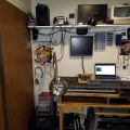
*edit - I was able to get the bypass logic tested with the 7" display, thanks to my new PSU. The mess of wires is getting more and more complicated and really need to figure out a good case. I keep looking at the Pactec PT10 but between that and the laser cutting order... Still need to figure out something better than a cardboard box
It was really exciting to see the 7" display test pattern and access the SD card. I had to slow the SD wayyyy down to get it to work with all the ribbon cables, but the display / SD (physically) works! I believe I've already found one error in my "test harness" logic, used an AND when I needed NAND.. I'm not sure about testing the display with this cpld bitstream but I'm hoping to test the SRAM and SD / SPI bus. The FLASH part should be enabled too, but I have no experience with the chip so getting signs of life from that will be very exciting.
I've spent some time testing SD / SPI bus as well as getting the SRAM working. I'm really happy with the design and being able to change the glue logic after the board was built is proving worth it's weight in gold. I'm still trying to find any optimizations, and since the software does the same thing so many times, it would probably be faster to have the hardware do it automatically... I'm hoping to have the full P2 TouchOS ported before Halloween, fingers crossed.
Got a couple apps I can't wait to develop with this thing. My #1 focus will be a MIDI interface / matrix module. I need at least 4 MIDI ports and 2 USB midi to glue my small studio together. Midi note data should be easy, heck I've used P1s for this before. I'm hoping to get MTC / MMC working, possibly MTC / Midi Clock sync. I see a lot of HIGH DOLLAR midi sync boxes out there and I think this could be a great app for the P2. Eventually I'd like to see if I can plug my Novation Launchpad into the P2 and get the USB HID working.
Joe
Yes, having a CPLD on there, means you could make the whole thing fast serial on the Streamers, if you wanted to.
There are Rasp Pi LCD boards that claim I think 128 MHz 125 MHz using a XC2 CPLD.
Those displays looked interesting enough that I picked one up some time back. I have not had the motivation to hook it up and try getting pixels out. I haven't actually tracked down the chips to see what they used but I could take a picture if you're interested. It's something like 4 or 5 soic14 or 16s or something. I happened on schematics when I was looking at playing with the thing but decided to build an adapter board, and still it sits. They look like an extremely viable option for simple touchscreen apps. So many interesting possibilities!
The next board revision I'd like to see about updating the CPLD from the Propeller. Really close to proof of concept on P1, honestly one function away from streaming a file off of SD to the CPLD. I just need to wrap my head around endianness and write a few lines to handle >32b registers.
With the streamers I should be able to run FAST @16b, although I can't wait to see what decimating the max clock does to the display and just how far I can push it.
That would be impressive.
If you are doing a board revision, ISSI show a MUXED Static SRAM, 4MBit IS61WV25616MEBLL, that could connect well to a CPLD, as it needs fewer pins connected.
A CPLD coupled to 4 x IS62WVS5128GBLL QuadSPI 45MHz SRAMs would also make for interesting memory, as the PLD can rapidly re-address 4-wide, and thereafter it just clocks out, streamer fashion.
I've been spending a lot of time trying to refine the "hardware debugging" option I've implemented in the cpld. It uses the 5 spare cpld pins to view various functions via mux. It caused me a lot of headaches trying to get the normal functions not to disturb the debug functions but I think I've got most of the bugs ironed out...
I still need to figure out the SPI for the touchscreen. I thought that /CS was not being activated but that was probably just a result of the "hacked in" debug functions. Once I get some code cleanup done it will be handy but caused a lot of tail chasing (the past 2 days!)
The cpld schematic is a bit messy... I had 2 extra bits in the latches and no idea what to name them so... Bip and Boop it was. There's still quite a bit of room in the cpld, although I'm laying out a new board which changes quite a few pins for physical routing.
Really excited to get the P2D2 in hand and figure out if my vision is going to work. I'm hoping to have the PortA pins accessible via right angle 2.54 male header on the p2d2 while it's plugged into my board.
Just a quick update for now. More once I get the spi fixed!
The touchscreen functions seem to work, although I haven't played with calibration yet. I need to write a program to find the limits of the touch panel and perform the calibration, all which will be part of "bios" file. The touch panel outputs a 12 bit value but the calibration matrix I'm using has a 10 bit limit IIRC. I could just shift of the LSB but that will lose precision and I'd really like to see if I can just subtract an offset from the raw values. I do a simple averaging on 2 x,y samples for debugging although I'm thinking of taking 3 or more and doing some statistical analysis before returning a sample.
The outer edges of the 7 inch displays have some weirdness to them (I never really examined the 3.2 inch displays outer edge sensitivity.) Say values are decreasing along an axis, at the very edge they suddenly increase. I'd like to examine this a little closer before determining the best way to handle. Perhaps someone would have some advice...
Touch.spin2 is shaping up at least. It's down to under 500 lines, but most functions are buried in the includes. The desktop app compiles and should just work (fingers crossed) once I finish the touch panel driver.
The touch.spin2 object and include section
OBJ
        str     :   "ASCII0_STREngine.spin"
        mod     :   "ymodem.spin2"

#include "HAL.spin2"
#include "touchStuff.spin2"
#include "RamStuff.spin2"
#include "displayStuff.spin2"
#include "FatStuff.spin2"
I do have a bunch of warning: Label is dereferenced with greater alignment than it was declared with but this is the way things are written. I might go back and try to make these warnings go away at some point but 11 warnings isn't bad.
The main reason I'm still waiting on handling the calibration is...
The 7" display I have now has a SPI flash chip I've been considering storing the calibration values on. Perhaps a font or two. All of this normally resided on the SD card, but with the flash chip I can store "display specific" info on the actual display board. This would handle the PnP display idea, where I was planning on reading the display controller to find out what kind of display is connected. This wastes a CPLD pin for something only to be used at boot though. I can't really find a compelling reason to read back info from the display controller other than at boot... maybe I'm missing something.
Another advantage is the BIOS program would be much smaller without including a font. Not so much of an issue for the P2 but I still plan on using this design with the P1 and every long saving there helps! I think I'm going to add a footprint for the propeller FLIP to this board. Or at least try!
Newhaven sells a line of LCD with EVE2 chips on the back. These cost almost the same as the LCDs alone. Makes it very attractive.
I have a P1 driver for these, but now with P2 hope to make a 4-bit (QPI) interface to make things much, much faster.
I've been thinking a lot about using the cpld/memory board for audio. The low overhead for address setup would make it ideal imo. With some optimizations to the current ram driver, I think a lot would be possible...
I've also been working on a board layout for the P2D2, still.. I'm actually kinda glad I haven't sent the artwork in yet since I starting looking at other SRAM chips tonight.. Given the speed of the P2 pins, 55ns SRAM is SLOWWWWW. There's some interesting looking 10ns SRAM but they have a different pin layout. I'm also thinking about adding a WX footprint.
AS7C316098A - 1024k x 16b 10-ns SRAM
https://www.alliancememory.com/wp-content/uploads/pdf/sram/fa/AS7C316098A.pdf
IS61/64WV102416DBLL - 1024k x16b 10-ns SRAM
http://www.issi.com/WW/pdf/61-64WV102416DALL_BLL.pdf
It looks like these have similar pinouts, although some of the address bits are labeled different? I think I'd like to stay with 1M srams, since I can load 19 address bits to the CPLD counters at one time. Some banking mechanism could be used to handle larger chips. Need to think on this some more. I'm also considering replacing the CPLD footprint with the xc2c256 100-TQFP that has a total of 80 I/O. I will leave pin compatible so the 64a can be used, but if I need more CPLD I/Os, it would be nice to just load the larger CPLD...
*EDIT
Looking at Xilinx devices shows an XC2S15 and 30 in the same 100-TQFP footprint. It also seems the FLASH part I used on the last board is Obsolete.
I've looked at the EVE2 displays a few times. They look really nice, and if I had a project that needed something right away I'd go that route. This is more of a hobby project, for my own sadistic enjoyment