

Prop2 Layout Viewer - Try it out!!!
 cgracey
Posts: 14,280
cgracey
Posts: 14,280
This is something really neat...
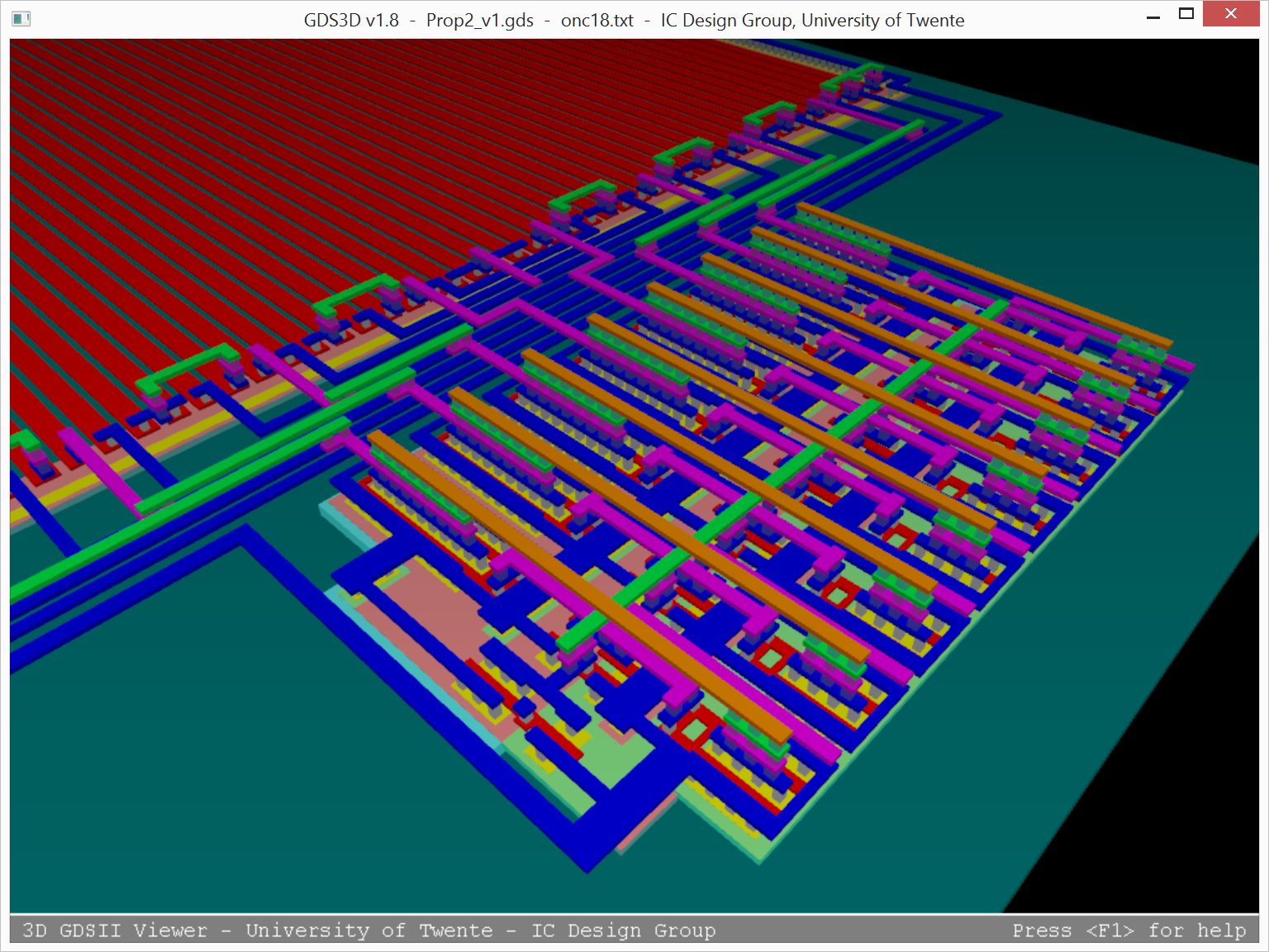
I got the GDSII layout file from Treehouse the other day and loaded into our Tanner EDA tool, which is a 2-dimensional layout editor. After examining it for a bit, I was thinking it would be great if I could see the layout in three dimensions. It turns out that a Dutch university made a 3-D GDSII viewer, and it's free! It really is snappy and very simple to use. It even has a trace function, where you can click on a wire and it greys out everything but the conductive path. And get a load if this: It's only 1.2MB - and that includes Windows, Linux, and Mac versions!!! I think it just takes the database and builds a world that your graphic chip renders from whatever perspective you select. It's 'live', like a video game, so you can fly through the layout at a 60Hz frame-update rate.
Download the viewer here:
https://sourceforge.net/projects/gds3d/?source=typ_redirect
Then, get this file that contains our GDSII layout and a setup file for the viewer:
https://drive.google.com/file/d/0B9NbgkdrupkHNGwyWS1WZFZCaWc/view?usp=sharing
Unzip that file into the same base directory that the GDS3D program resides in. Then type this, if you're in Windows, to run it:
win32\gds3d -p onc18.txt -i Prop2_v1.gds
Hit F1 to get a keystroke menu.
You can see every cell in the padframe, and even select them, individually, and view them in isolation. This program doesn't show text labels, just polygons. For anyone who's interested in what a layout looks like, this is a goldmine. This is all full-custom, from schematic, so it is quite sensible to look at.
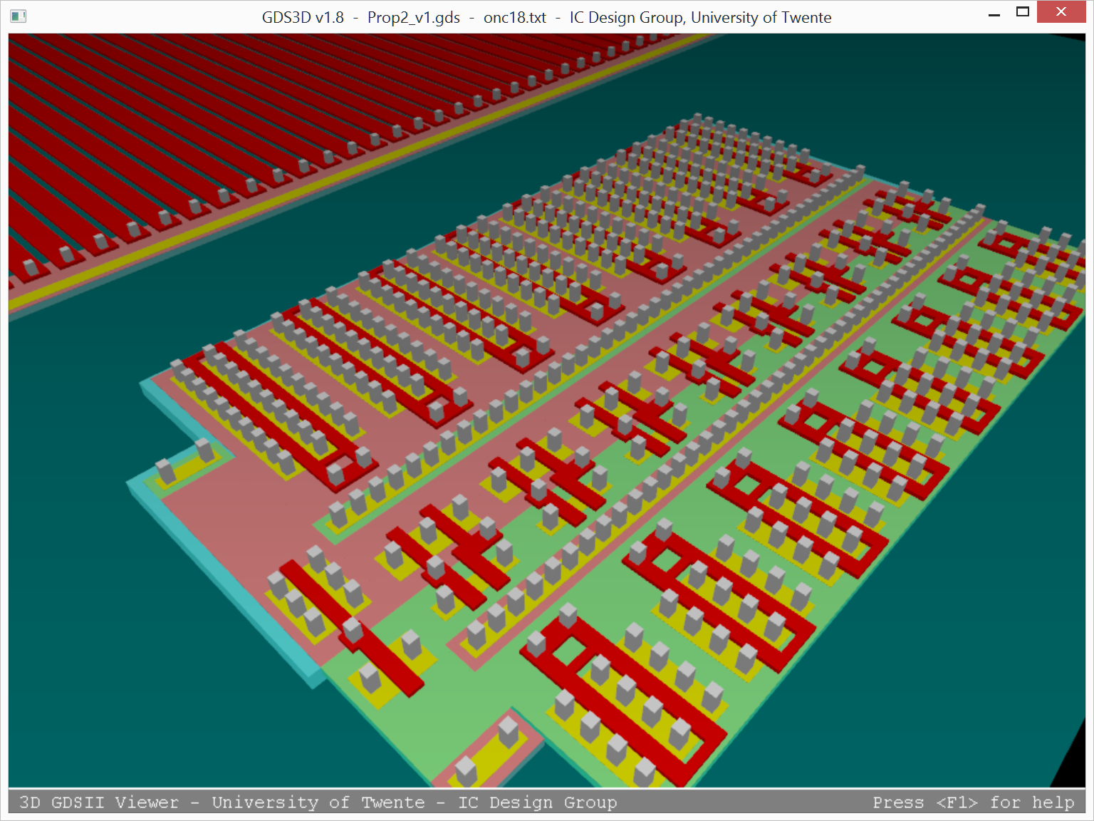
Here is the THICK_DAC_SLOW, an 8-bit R-2R DAC that is in each PAD_IO and feeds into a comparator for I/O pin level sensing. It uses common-centroid resistor layout for precision. Those red lines are poly resistors that are about 1k-ohm/square. Being ~50um x 0.75um, they are about 67k-ohm each:
Here is a view showing N-well, P and N implants, active, poly, and contact layers. Can you spot the NAND gates?
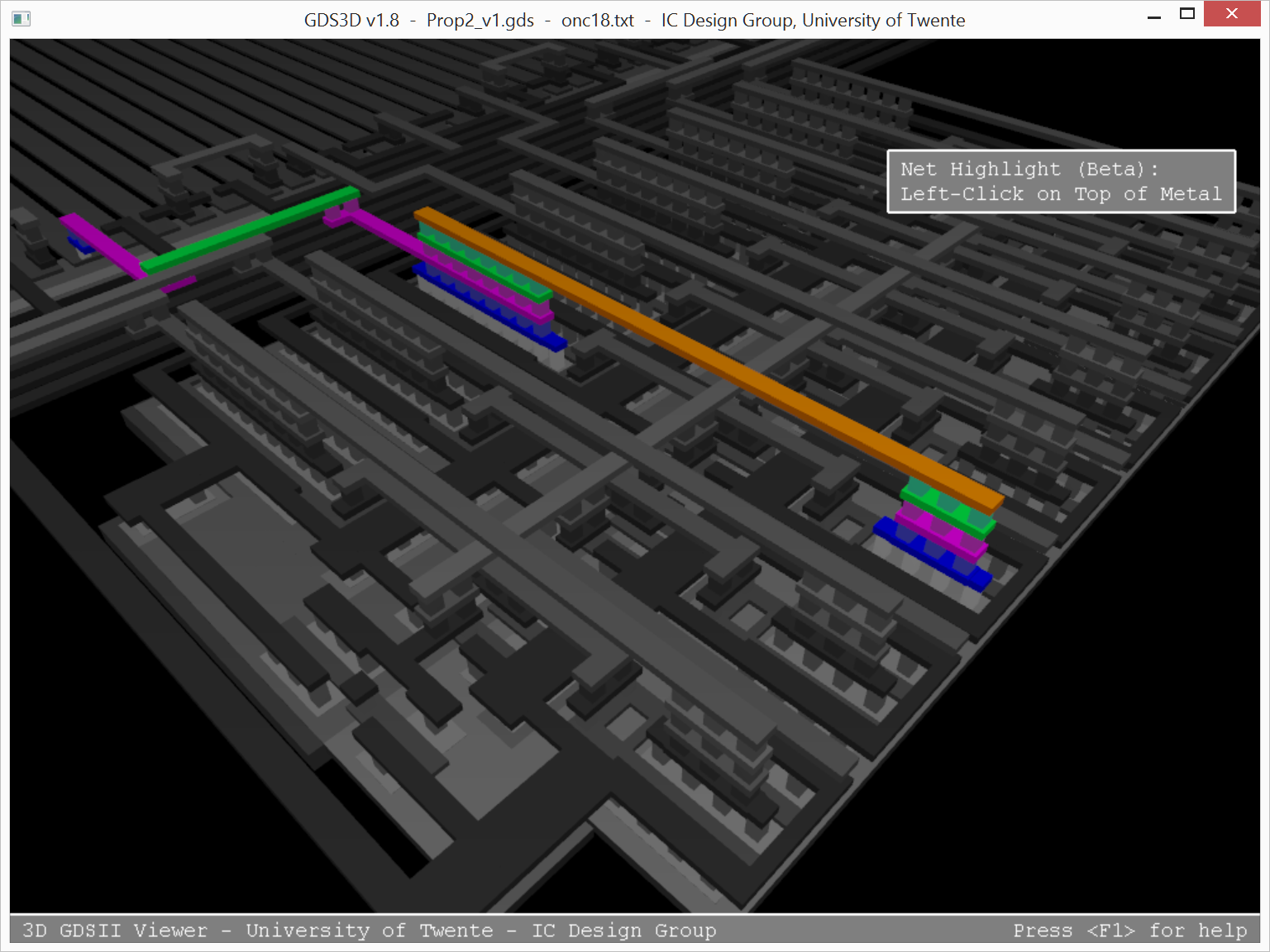
And here is a trace of one of the split inverters' outputs that drives a resistor in the R-2R network. That's a lot of jumping around. Who's going to drill all those vias?
It's nice inside these ADC's. Does it ever get hot in here?
I got the GDSII layout file from Treehouse the other day and loaded into our Tanner EDA tool, which is a 2-dimensional layout editor. After examining it for a bit, I was thinking it would be great if I could see the layout in three dimensions. It turns out that a Dutch university made a 3-D GDSII viewer, and it's free! It really is snappy and very simple to use. It even has a trace function, where you can click on a wire and it greys out everything but the conductive path. And get a load if this: It's only 1.2MB - and that includes Windows, Linux, and Mac versions!!! I think it just takes the database and builds a world that your graphic chip renders from whatever perspective you select. It's 'live', like a video game, so you can fly through the layout at a 60Hz frame-update rate.
Download the viewer here:
https://sourceforge.net/projects/gds3d/?source=typ_redirect
Then, get this file that contains our GDSII layout and a setup file for the viewer:
https://drive.google.com/file/d/0B9NbgkdrupkHNGwyWS1WZFZCaWc/view?usp=sharing
Unzip that file into the same base directory that the GDS3D program resides in. Then type this, if you're in Windows, to run it:
win32\gds3d -p onc18.txt -i Prop2_v1.gds
Hit F1 to get a keystroke menu.
You can see every cell in the padframe, and even select them, individually, and view them in isolation. This program doesn't show text labels, just polygons. For anyone who's interested in what a layout looks like, this is a goldmine. This is all full-custom, from schematic, so it is quite sensible to look at.
Here is the THICK_DAC_SLOW, an 8-bit R-2R DAC that is in each PAD_IO and feeds into a comparator for I/O pin level sensing. It uses common-centroid resistor layout for precision. Those red lines are poly resistors that are about 1k-ohm/square. Being ~50um x 0.75um, they are about 67k-ohm each:
Here is a view showing N-well, P and N implants, active, poly, and contact layers. Can you spot the NAND gates?
And here is a trace of one of the split inverters' outputs that drives a resistor in the R-2R network. That's a lot of jumping around. Who's going to drill all those vias?
It's nice inside these ADC's. Does it ever get hot in here?
Comments
IKR!?! Now, if only I knew what I was looking at...
Are those little grey boxes where you load up the magic smoke?
Thanks for sharing
Sadly it does not work here.
Compiles fine on this Debian x86-64 but:
No Mac or Windows?
Ick! The controls are all backward. Time to use that source code ...
I need to drive all through this thing and identify places where the routing needs beefing up. This passes LVS (layout vs. schematic), but there are some big loads, like those PMOS and NMOS devices near the bond pad, that need a lot more power and ground metal going to them.
But sure enough the prebuilt binary works.
That really is awesome.
Now to hack it up to export all those rectangles as babylon format and we can view it the web.
Get used to using ctrl-mousewheel to disable and enable layers in sequence. It's really handy.
Hit "T" and try going into the various blocks of PAD_IO. There's lots to see.
"make bininfo" on the original tells of needing libpthread.so which doesn't show up in the quick recompile. It's also 32bit.
Chip, in your third piccy - split inverter, How come there is so many layers there just in a straight up vertical stack? And what's with the multiple sandwiched cubes?
Is this the hardware equivalent of machine code viewing, the schematic conversion to physical constructs.
A s(t)imulation of this model showing the various wires and elements switching would be the next step, though if such things exist I suspect they are big money?
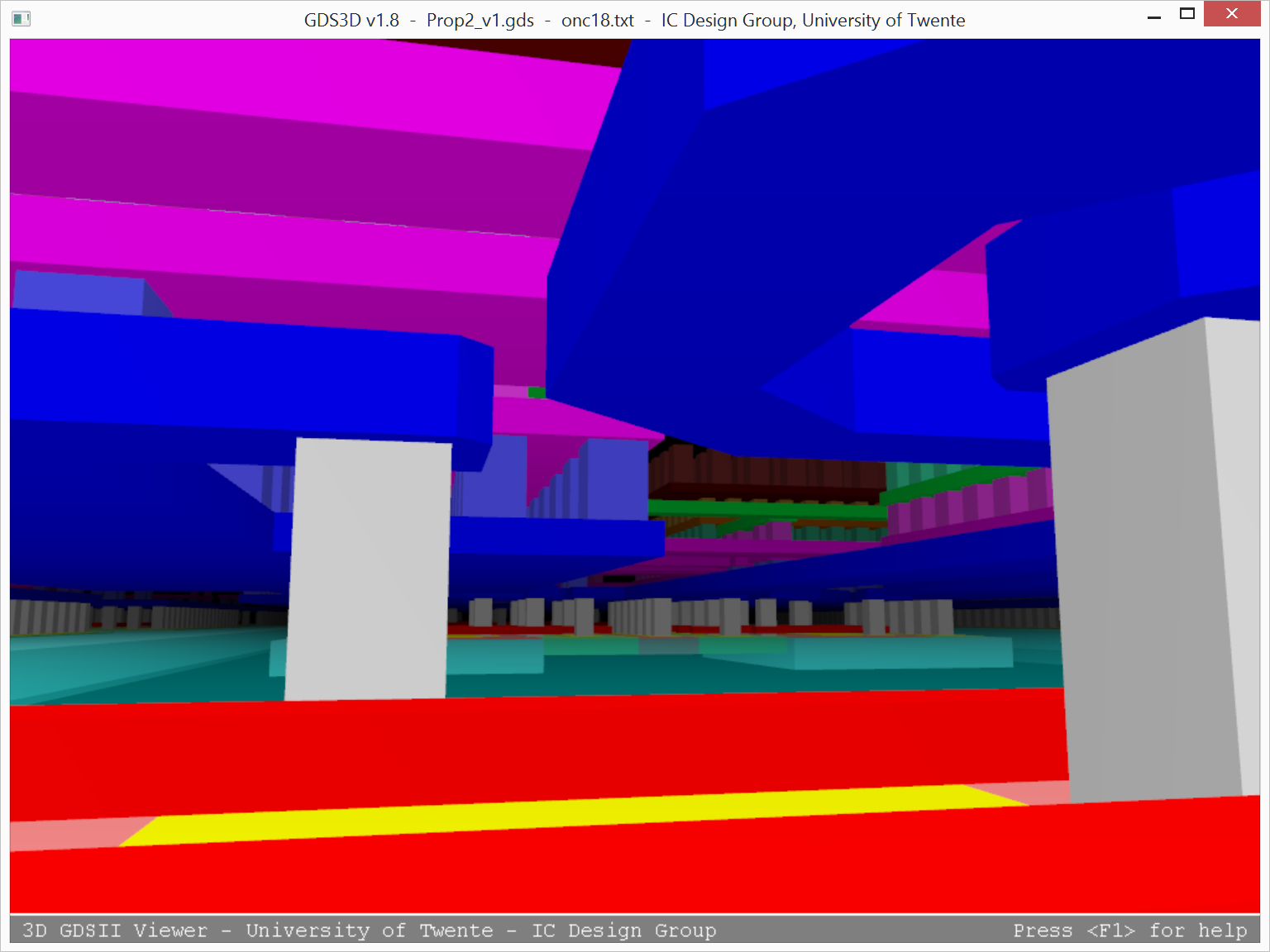
Those cubes are vias. They are drawn as squares, but wind up round after fabrication. They are interconnects for the metal layers.
In this case, the layout guy just decided to use even metal layers for running wires one direction, while odd layers were used to run wires perpendicularly. You can see how, by breaking that rule, you could save a whole layer of metal. That's going to get optimized. We should see an improvement in the next layout, which will be done in two days. I'll post it here.
That's a very nice picture of an inverter. You can see the cyan N-well, in which the PMOS transistor is built. NMOS transistors are built right in the substrate. In each case, there are some P+ and N+ implant areas. In digital logic, PMOS transistors' poly gates (red) are always 'wider' than the NMOS transistors' gates, since they are not as conductive. The gate 'length' is actually the narrow dimension of the poly that divides the active area (yellow).
I don't know that such a simulation tool exists, though I'd like to make one. If only chip fabrication weren't so expensive, there would be a nice market for such a thing.
What you are seeing in that GDS3D screenshot is the mask data drawn verbatim in 2-D, and then extruded into the Z axis to show what the fabricated chip will be shaped like.
Imagine all those right angles being smoothed away and you'll have an idea of what actually winds up existing:
Look at this picture:
I have to unpack my laptop and download the program and files and get my hands dirty.
There seems nowhere else where you can this sort of education outside of real jobs. Hats off to Chip and Parallax for allowing us to participate!
Set the top cell to PAD_IO, CTRL+scroll down until all layers above M3 are invisible, and then zoom in on the square pad on the top.
This next image is with only layer M3 visible, viewed from underneath. You can see it's not rectangular, not to mention the Z-buffer glitches due to coplanar polygons.
The problem could easily just be my computer, a 2009 Macbook running Gentoo Linux with an Intel GMA GPU that probably has bad drivers.
EDIT: If I set the top cell to PAD_BASIC, it goes away. But it consistently comes back if I look at PAD_IO.
I think there was a spare decode slot, and IIRC you have Nett=15pf and Nett=30pF lines, but no Nett=PinC for lowest Cap crystals, or Clipped Sine feed cases.
More steps would be nice, but I can see that is more work ? 3 should be simple.
3 CL Steps also allows some correction action, where you target the mid value, and then measure and nudge CL values Up/Down using the other 2 choices, to trim for long term 'zero-drift'.
This can also allow deliberate clock modulate for sampling, to avoid exact sync effects.
Did you look at the PLL Counters, and allowing (Crystal / M) -> PFD = VCO/N ?
Present PFD= crystal, is quite restrictive in VCO choices.
A 5 bit Crystal divider keeps PFD in the MHz + region, & gives 8-9 bits VCO div.
Examples :
you can generate a USB related 48 or 96 or 144 MHz from a low cost GPS 19.2MHz Clipped Sine TCXO
or, you can use 19.2 or 26MHz GPS TCXOs to PLL to an exact 100.000MHz
- That's not possible with PFD=Crystal.