

Propeller 2 I/O pin infrastructure
 JDat
Posts: 103
JDat
Posts: 103
Sorry, if it's already discussed, but I can't find on forum.
What about P2 I/O pin functions.
Will there be following functions:
1) Internal pullup
2) Internal pulldown
3) Open Source to GND
4) Open Drain to VCC
5) Push-pull VCC/GND
6) Input
7) Schmitt trigger input
8) Alternative function (ADC input)
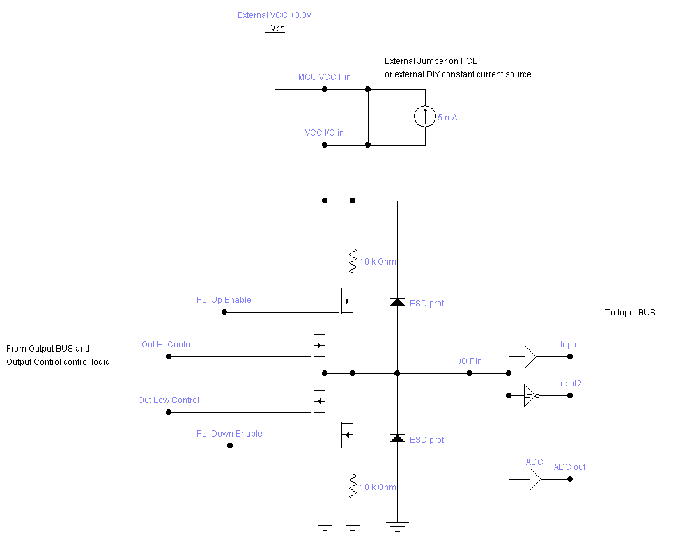
VCC I/O pin.
See Attached Schematic:
What about P2 I/O pin functions.
Will there be following functions:
1) Internal pullup
2) Internal pulldown
3) Open Source to GND
4) Open Drain to VCC
5) Push-pull VCC/GND
6) Input
7) Schmitt trigger input
8) Alternative function (ADC input)
VCC I/O pin.
See Attached Schematic:
Comments
There are plenty of designs where Open Drain is good, that do not also need outside the rails.
This becomes more important where Serial hardware support is added.
Examples I can think of are i2c, where the spec calls for open drain, and keyboard scan apps, where open drain with PullUp/Down choices, safely tolerates multiple key presses.
Chips often also disable the Input buffers, so they do not draw current when not being used.
Some chips have a choice of TTL or CMOS logic levels.
If there is to be no choice, a lower threshold that allows 1.8V direct drive would be more useful.
(the ADC manages the Analog side)
IIRC Chip did talk about a current-source mode, with some user control of current.
I've got the delta-sigma ADC improved quite a bit from the previous design. It now uses very high-impedance current sources and sinks, internally, instead of resistors, to make a much more linear signal path and integrator. I just finished it yesterday. At least, I feel that it is finished. That took almost a month and it was like travelling down a 5,000 foot mineshaft. There are so many subtleties in such circuits that need a ton of attention to get right.
I'm going to revisit the DAC tomorrow and I think I might change it around so that instead of always outputting a 75-ohm rail-to-rail voltage, I'll add a current-source-only mode that will enable you to locate a load resistor to GND outside of the chip, cutting the power dissipation from 40mW down to 20mW. That seems like an awful lot of power, but to switch accurate analog levels quickly, it takes juice. There's no time for feedback loops. It has to run open-loop and settle in a couple of nanoseconds.
Aside from the ADC and DAC, all pins will have current and resistance output modes of 1mA, 100uA, 10uA, 1k ohm, 10k ohm and 100k ohm. You can configure pins for open-source/drain operation, too. For input, there is logic-level, Schmitt, pin-to-pin comparator, and 8-bit level comparator. There are some other modes, too, but I'm not on my work computer at the moment, so I can't see everything.
I would like to make a post soon about the ADC, because I think it's pretty neat and you all might find it interesting. I learned a lot of new things about current-mode circuits. They are to voltage-mode circuits like inductors are to capacitors. It's a whole different set of paradigms to work in. I think I got the circuit designed well, but I just ventured into that domain to do a job, and I can see how many engineers could spend their whole careers just doing ADC design.
Most all complex chips today are made by integrating a lot of separate IP blocks, including I/O pads, with a big blob of synthesized logic. It may seem silly to design our own ADC and DAC (and I/O pins), but to get circuits that do what we need and are very compact, we're stuck doing this. I think the results will be good.
Forgive my ignorance (which doesn't stop me from being curious), but does anyone know whether that "load resistor" is per I/O pin used in the c-s-o mode, or per DAC or DAC-pin, or chip-wide. And would such a pin connect directly with an I/O pin or be implemented through a separate configuration pin that only sets up the load impedance elsewhere internally? Okay, forget all that: in the case of 75 ohm VGA video, where would that load resistor (or those load resistors) be located? I'm presuming that there would there be a separate load resistor hanging off each color channel (RGB), but maybe I'm wrong.
Changing gears entirely, I can't help but wonder if a scaled-down digital-only version was ever contemplated for applications that don't need A/D (though some "simple" form of internal D/A might could still be nice). A digital-only version of the chip could be used to test (beyond FPGA tests and other simulation) the digital functionality of a future analog-capable chip and seemingly could come (or more likely "could have come") to market months before an analog-capable chip. However, at this point, the release times (if there actually were a digital-only design in the pipeline) might very well be the same, as it seems that Chip is already well down the analog path. On the other hand, who knows what complications might crop up with the analog features (pre- and post-design). Hopefully, the digital portions of the chip will be unaffected by any such potential issues (such that any sample or mass production chips could still be used in some apps). Anyway, a second design would really up/increase the fab costs, wouldn't it!! Moreover, the new chip will especially shine in terms of its analog capabilities, Oh well, I was just musing/wondering.
The I/O modes still sound nice. Sounds like can do direct USB...
Both voltage and current modes can be good.
For video, I see most DACs use current and we have seen benefits in that, especially on larger logic devices.
Current DACs give you some Power supply rejection ratio, and also decouple you from ground noise inside the device.
On real displays, noise from both those sources can be visible to a critical eye.
For general purpose use, a voltage DAC is easier for most to understand.
Is the 4th unstated value here used for full drive ?
1mA is a nice round number, but perhaps a little light. Can these be globally set ?
3~5mA are perhaps better for LED and direct NPN base drive, so a Decade choice, with a global base would be good. Much above 5mA is going to be adding power issues.
Will the threshold choices allow direct 1.8V logic drive IP on 3.3V Powered groups ?
( that needs other than 50% CMOS level)
Do you mean from the "pin-to-pin comparator," mode ?
USB also needs a differential driver, and some logic support for the signaling states would help too...which I did not see explicitly mentioned. Then there is the sense resistor ...
What conversion speeds / clock rates and precisions do you expect this ADC to offer ?
There are also a growing family of isolated delta-sigma ADC's, that use 2 pins, CLK and Data.
- see Analog Devices, TI, etc
Some provide the CLK and some (most?) receive the CLK and echo the Data
I see ADi have a LVDS version, RxCLK, specs 20MHz sampling clock -- looks like they use LVDS to lower the circuit noise.
Avago have an opto version with TxCLK(~10MHz)
It would be good if those could be supported, in a mode feeding into the ADC totalisers (and filters, if any). [ CLK, CE ?]
I would expect an on-chip ADC to have a reasonably high noise floor.
The Prop1 can support them already in a basic sense. There is two variations for clocking: Either use the Prop as the clock source or just run everything asynchronously (Only the singular data pin needs to be coupled) with the Prop totalling at 80MHz to easily beat Nyquist limit.
Prop2 will at least have this capability as a minimum.
RxCLK case I am less convinced of, as imagine a idle zero (50% duty), and then as that phase-drifts, when the edges timing hits internal sample points, there will be an aperture jitter effect.
I think RxCLK needs a counter (or filter) with CLKin and CLKen.
It's seriously oversampled analogue information, jitter is actually good for precision. A coupling clock signal is not required at all.
The good news with the synchronous method is only one clock source is needed. So, if one of the Cog's counters was used then all of the remaining 15 counters are still up for grabs.
The correct digital information is encoded in the centre of the data bit, sampling on the data-bit-edges is NOT a good idea. Even modest skews (1ns) and beats, can drop precision to under 7 bits.
I suggest you tell that to Avago and Analog devices et al - you could save them wasting a pin and some complexity
We're well above Nyquist at 80MHz totalling on the Prop1.
With synchronous clocking the circuit can perform all functions at optimal spec so long as things like ground bounce don't interfere. With asynchronous clocking a minimum of double bandwidth is required. The Prop1 has more than that to spare in it's counters so it can function asynchronously.
The take-home point, for P2 I/O (back to the thread topic) :
Those expert analog companies do put two pins on the parts for a good reason, ideally the P2 will be able to use both pins, in both RxCLK and TxCLK modes.
Nice progress on ADC.
As someone pointed it have be good to have one 2 pins to one differential output and one 2 pins differential input to one pin Input same in both cases as USB have)