

P2-Eval LDO Oscillation - No CL
 jmg
Posts: 15,148
jmg
Posts: 15,148
in Propeller 2
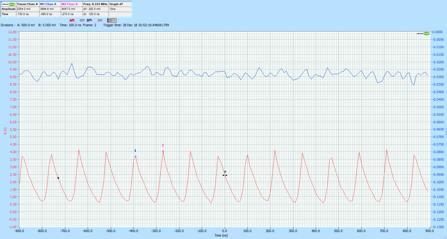
As I feared, the no CL PCB layout has the LDOs not stable.
This means you should not connect external circuits to the 3v3 labeled pins, without adding a large enough decoupling cap.
When the jumper moves on the PCB, the fitted cap is then connected to the LDO, so it should be ok.
Scope captures show the oscillation at no load, and at 40mA ( At 2mA it is even worse)
No load oscillate is a 200mV at 245kHz signal, that might be ok, but it's probably not helping the noise floor of the total system having those all squarbling away.. ?

1478 x 793 - 72K
1478 x 793 - 106K
Comments
Are you saying not to use the VIO power on each I/O header?
In the case of no-load, the 200mV must be related to the measuring technique. An unloaded LDO of this type will not exhibit such ripple, and more importantly, will not impact VIN beyond the VIN cap. Ie. with the LDO output disconnected, it is not connected to anything and will not squarble anything.
I believe this is a red herring.
-Phil
Sounds a bold and sweeping claim - have you actually applied a scope, to check such a claim ?
CL is the load capacitance such LDO require for stability. The PCB is designed such that CL is missing from the LDO, until the jumper is moved.
No, just that it needs care around the pins labeled 3v3 on the board.
It may have a LDO regulator, and be labelled 3v3, but that is only for jumper-to-P2 special case use (adds the CL)
A general user might expect a pin labeled 3v3 from a LDO to mean it is available as regulated 3.3v (eg to power a oscillator module)
I was going to add a 1/4 watt load resistor today and see if it improves things
This is all part of "the learning"...
The 3v3 SMPS cycle skips at low loads, and seem to need ~ 100mA (33R) to change to every-cycle regulation.