

P2 Floppy Drive Controller
 rogloh
Posts: 6,414
rogloh
Posts: 6,414
So here's an old school project for the P2... ![]()
I have just finished designing a PCB for the P2-EVAL which in theory should be able to read/write from old floppy disks using a P2. I did this as I am intending to eventually have a full P2 emulation of a Microbee Z80 machine from the 80's (for another project) and as part of that I want to be able to figure out the floppy disk interface using a P2 and then create some disk images from old floppies I own. Or I might potentially even keep this same HW design present in the final emulated system connected up to real P2 IO pins (along with a Z80 PIO chip). So this is both a learning exercise for me and a tool at the same time.
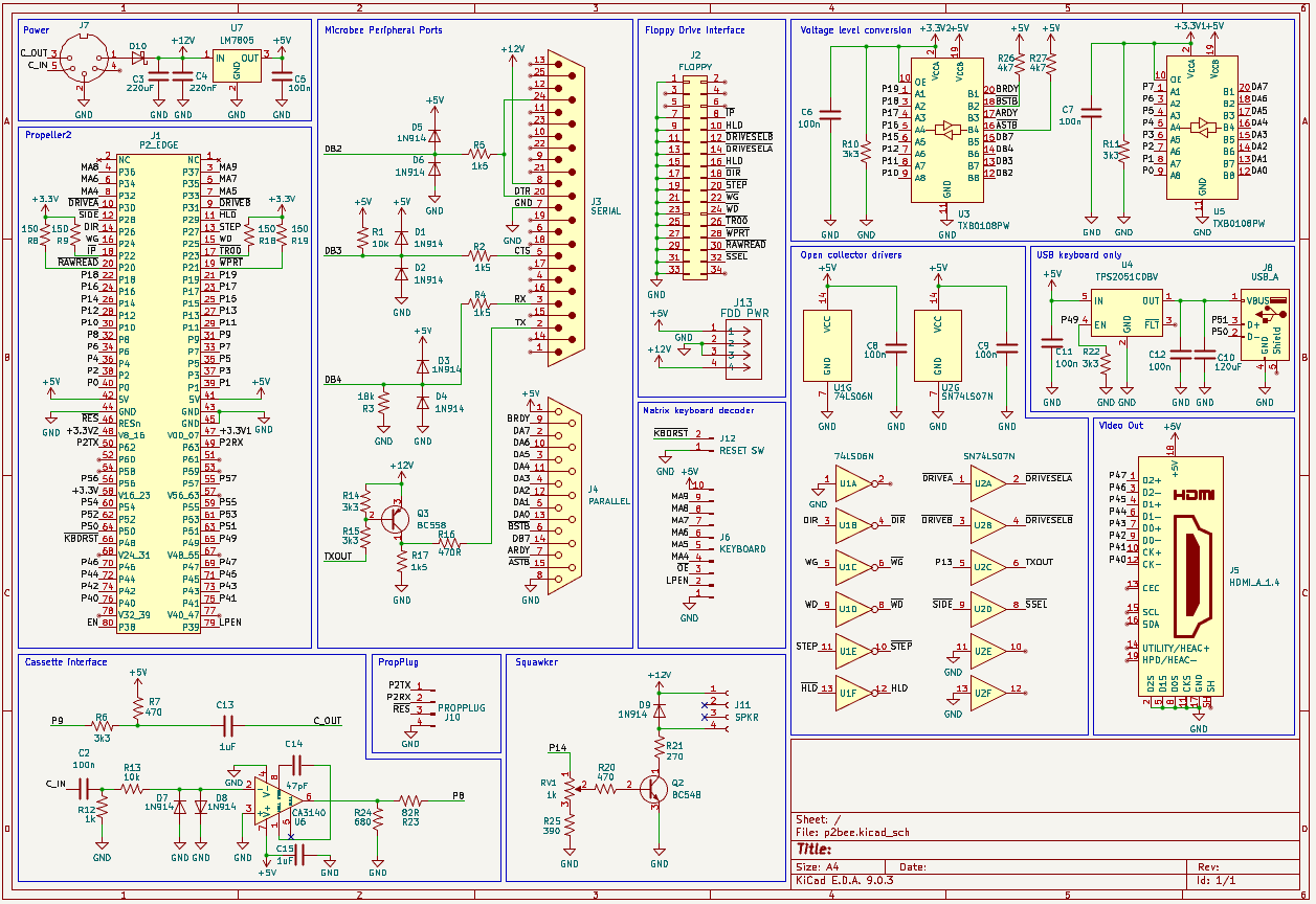
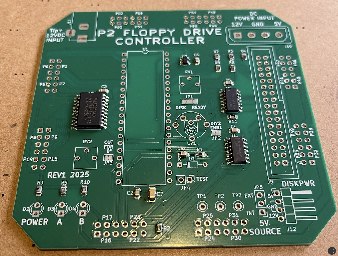
Here's the board render (a few parts are missing their 3D models). It uses a WD2793 controller chip as the core component and interfaces to the P2 using typical async bus signals with some 3.3V level conversion on the data bus towards the P2 using a 74LVC245. The other parts are just 74LS open collector drivers which drive the floppy disk and handily also work with 3.3V control signals where needed.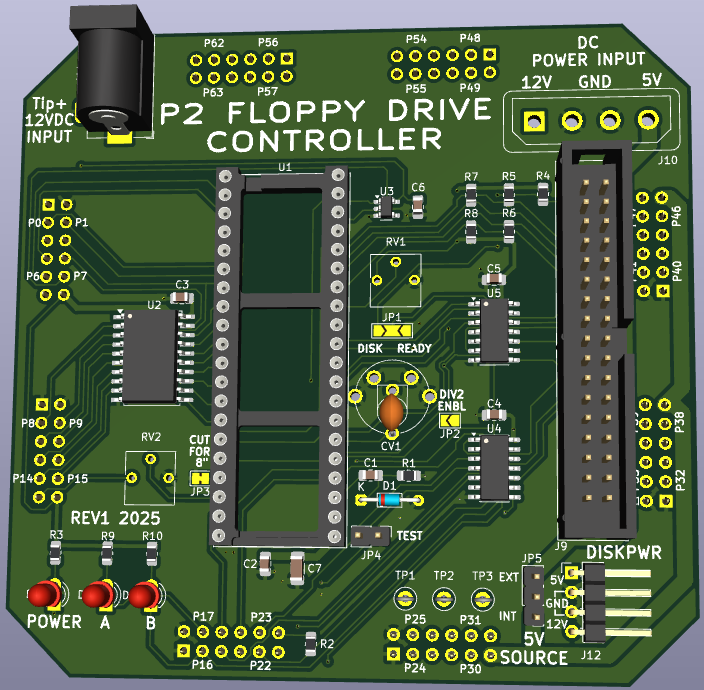
The disk drive's power can be sourced by an external 5V & 12V DC supply using a typical 4 pin Molex receptacle which gets passed through to the 4 pin Berg connector for the 3.5" drive. There is also an option for feeding 5V only from the P2-EVAL with the extra 2A USB input source in cases where 12V is not needed (e.g modern 3.5" floppy drives), or another scenario where 12V only is input via DC barrel jack and 5V gets supplied by the P2-EVAL. This board and controller will probably even work with the older 5.25" drives too, with suitable power cabling adapters (Berg to Molex) although that is not my own application.
The schematic is provided below.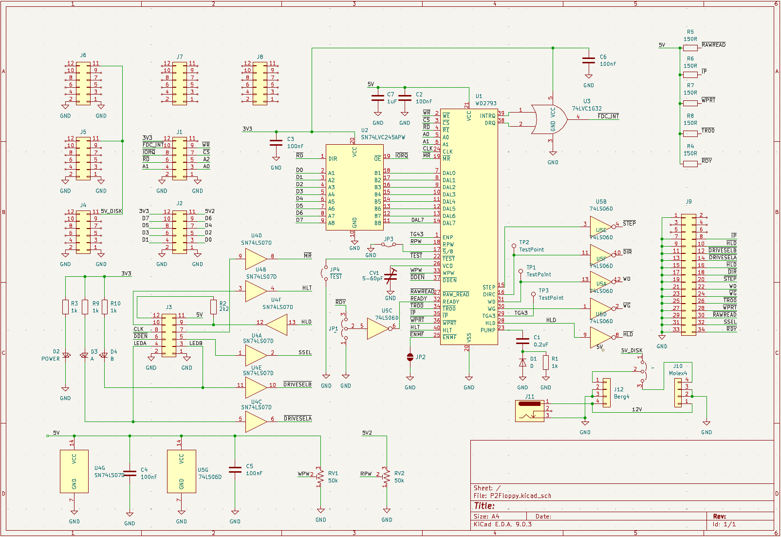
The PCB should get made in the next few days with help from @Tubular and I may see it back next week with any luck. Probably need to think about component ordering now...
If there's any interest from others I may decide to share the KiCad design files, although sourcing the older parts is not that easy, particularly the controller, and even the trimmer cap (which seems to be getting more obsolete these days, not surprisingly with the whole digital revolution we've had).
Cheers!
Comments
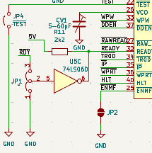
Ooops, last minute fix. Needed a pullup resistor on one open collector output driver to the READY input. Luckily the board had not been fully submitted (was just about to be according to Lachlan) and I could fix it in 5mins. Doh! Other o/c signals have pullups inside the WD2793.
I'd think the Prop2 can do the MFM encoding too. Don't really need the WD2793 do you?
Err, hmm, it's not the encoding that is the problem is it? It's the variable read back rate that has to be sync'd and locked to on the fly. That needs the right front end. Like with the Ethernet phy chips.
Yeah I was thinking that at some point I may consider that option to control the floppy disk directly from P2 IO pins. Maybe once I learn more I might try that idea out. That would be a nice way to reduce HW even more. In that case I could have a setup with the Z80 PIO also fully emulated inside the P2 and just bring its IO out directly from the P2 with minimal external HW apart from some voltage translation perhaps.
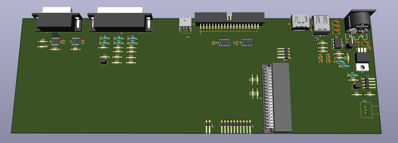
For now I've taken an intermediate step first where I still include some old HW at the periphery. Below is what I've been contemplating for IO pins. It's a nice setup that fully uses the P2 and would expose the floppy disk plus the parallel and bit-banged serial via the PIO. Just the same as the Microbee. Video is generated by the P2 and a real keyboard matrix is scanned for presses or a USB keyboard version which is what I have running today could be used instead. The exact IO mapping below is not important for now but it's the total number of IO pins that is required here to see what fits and is feasible. In some ways it's just the same board as above with the PIO and its extra signals on other pins and a couple more connectors.
P0 ~IORQ
P1 ~RD
P2 ~WR
P3 A0
P4 A1
P5 ~CSFDC
P6 ~CSPIO
P7 FDC_INT (OR of DRQ and INTRQ - is polled by Z80 software)
P8..15 D0..D7 data bus to both PIO and FDC
P16 3.375MHz CPU CLK to PIO from P2
P17 1MHz CLK to FDC from P2
P18 HLD from FDC (for one-shot motor/head control)
P19 HLT to FDC (to know when head is loaded)
P20 ~DRIVESELA
P21 ~DRIVESELB
P22 ~DDEN (double density enable)
P23 ~SSEL (side select)
P24 ~MR (reset of FDC)
P25 - KBDRESET (for NMI signal)
P26 ~INT from PIO
P27 ~M1 to PIO
P28..P31 (SD card filesystem)
P32..P39 (HDMI or VGA+audio)
P40..P47 (Keyboard scanning matrix for 64 keys)
P48..P57 (8 bit PSRAM)
P58..P61 (boot flash)
P62..P63 (prop plug)
Update:
Actually looking at the above mapping makes me think a P2-EC32MB might be able to do a full Microbee emulation if I move to using a USB keyboard and either boot off SD and also use it for CP/M files or perhaps use the 16MB flash for an internal filesystem. In any case I might still be able to run the emulation without any PSRAM so a regular P2-Edge could be used too with more pins freed. This bodes well for a very compact final board and saves me needing to layout a P2 for high speed operation if it can make use of a P2-Edge directly off a connector at the side. I like that.
A fascinating project! The first Shugart drives 8" had the control logic and the controller was a board of same size, but could handle up to three drives. Then the FD1771 https://en.wikipedia.org/wiki/Western_Digital_FD1771 arrived, allowing us to fit a controller to a Europe Card format. And then there was the problem to sync with the double density encoding, as there was no separate clock signal (NRZ modulation). It's fun to see such a project arriving!
Yeah this controller apparently even suits some of the older 8" drives as well and in fact the FDD interface the Microbee uses is indeed the Shugart standard vs the IBM PC standard (a slight variation in selection of drive selects and other minor details but I was still able to use a modern Sony 3.5" FDD on the old Z80 machine with some simple wiring mods and cable twists). I've added both A & B drive selects for this project so hopefully two drives could work with it using the whole cable twist thing - the single motor on signal is still shared FWIW, but the two drives would have different drive select signals - the Microbee actually has 4 and used a couple of different pins to the FDC for selecting drives C&D and only one motor on signal. With an open collector bus no real electrical dramas happen if multiple drives try to output their data at the same time - it just won't work.
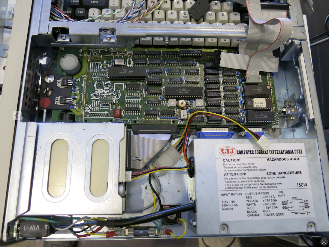
Here's a pic of old my Microbee (I transplanted into a old PC case) showing the floppy disk interface.
I also have plans to add a Gotek floppy emulator which I have kicking around somewhere to this too but that will also still need the same floppy disk interface to write images to.
MFM encoding can be done with some simple shift and bit masking logic. Should be no problem. MFM decoding requires locking to the incoming signal of which the frequency varies with the speed of the motor, excentricy of the disk and so on. But I think even this is no real challange to the P2. It should be able to do that in software combined with smart pins. All you have to do is to measure the time between incoming pulses to decide whether it's a 1 or a 0 symbol. IIRC, MFM puts an edge on even clock phases for 1s and on odd phases for 0s. So the spacing is nearly 2, 3 or 4 clock periods with some tolerance if the clock is twice the bit rate or 1, 1.5 and 2 if it's equal to the bit rate.
I've never really tried to think about it ... I've just looked up SD and DD floppies and found they were recorded at only 250 kHz carrier. That's quite long for the Prop2, enough time to massage things for sure. I might have to get inquisitive ...
Cool")
These two projects might be of interest if you ever decide to get to that low of a level on the P2 with this:
https://github.com/keirf/greaseweazle
https://github.com/adafruit/Adafruit_Floppy
Interesting projects @avsa242 . You know I wasn't thinking like this during the PCB layout stage, but for my board above I could have also brought out the applicable floppy drive side read signals to some P2 IO pins as well. Then I'd have access to read data directly read off the disk. But being O/C I can probably just mod the 5V pullups to use 3.3V instead and also blue wire them over to the IO pins nearby at P48-55. Maybe even the P2 internal pullups could be used instead, although they seem to show 150 ohm resistors in the Microbee design which I simply replicated here. I might try that out if I ever want to record flux transitions or at least observe the data at the low level.
Just tossed a pile of ancient floppy disks…
Maybe was a mistake…
I think the Amiga has used the blitter to do MFM encoding. On the P2 you could spread the bits with the MERGEW command and insert 1 bits where both neighboring bits are 0 with a logical NAND operation.
I'd heard that too. If true then it would've been easy to create invalid write encodings that made the magnetics weak for those copy protection schemes.
Yes, it also meant that the amiga could read all different floppy formats independantly of the controller chips used in other computers.
The best copy protection I heard of was writing a "wide track" with an old 40-track drive. You can read it with a 80-track drive while stepping the head position motor forth and back without corrupting the data. You can never write that wide track consistently with a 80-track drive.
Most of the active components for this project have been ordered from Digikey and were shipped Friday. So I'll have the key parts (and board?) next week with any luck, while other stuff I can get locally or have in here my spare parts bins. I will still need to source a legit WD2793 somewhere however so until then I'll need to temporarily re-use the original IC from my real bee and hopefully not trash the device in the process. The cheap IC's I found online do appear quite likely to be counterfeit by the look of the font and missing copyright symbol in the photo. Other chips I found from sellers from US or UK seem rather pricey to ship here but might be more authentic, not sure.
I expect I will use the original Microbee disk boot code in my emulator and map the applicable FDC related ports already being decode in software to trigger Z80 style IO transfers from the P2 IO pins using the actual WD2973 HW. That was the last part of my emulator that was failing to work when I tried to emulate the chip itself, and needed to be bypassed temporarily to let me boot and run programs I'd imaged previously.
So for a laugh while waiting for my boards to come back I messed about in KiCad and hacked up a minimalist Microbee circuit design that would use a P2 Edge as the brain which emulates the Z80 and yet retains the existing 5V peripheral IO & connector compatibility externally. This P2 emulator would need to simulate a PIO and FDC (if possible). If that turns out too difficult I would go back to the design that includes these chips on the board and then control the HW via actual IORQ bus signals generated by the P2. But a minimal variant is tempting to target. I already can run a working emulated Microbee inside the P2-EVAL (without floppy or PIO capabilities) which plays games and runs CP/M etc.
I kept most of the original IO pin mapping but took a couple of liberties in the design by adding the B channel strobe and ready signals on the unused parallel port pins (at least for early implementations), which would allow bi-directional mode operation. Also I added HDMI output for video (instead of composite) and USB-A port (for either a keyboard or a mouse or joystick perhaps). These connectors make use of the empty "user port" cutout on the back of the Microbee case. For convenience I also added a power output connector for a floppy disk drive next to the IDC header. The cassette interface is also still present on the DIN connector.
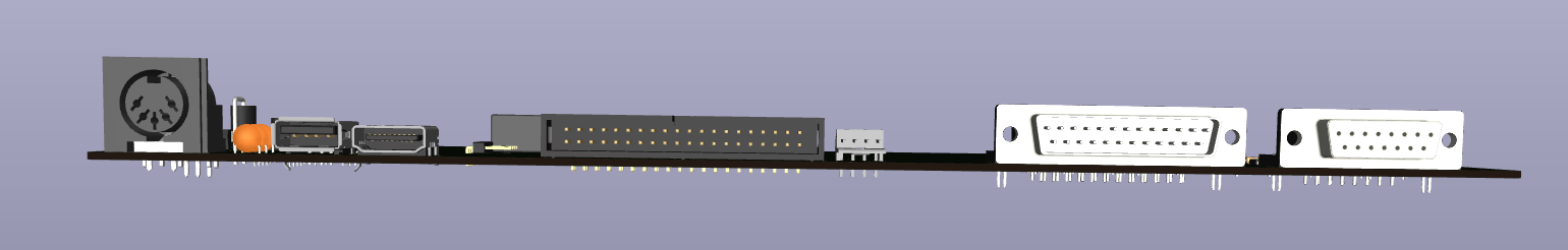
This 3d render of the unrouted PCB shows the general idea of what something like this might look like. I'd probably have to tweak this a bit more but still would want to use mostly through hole stuff for keeping that retro feel and ease of constructing it manually.
Here's my old crusty 'bee case (which could benefit from some cleaning and Retrobrite action), showing the position of the IO connectors. The PCB would fit inside the case (with suitable mounting holes in the right places) and the matrix keyboard that already sits inside the case would be connected as well. I really want to reuse the keycaps from my original keyboard and refit all the keys with modern day keyswitches - problem is that the keycaps need some stem adapters to attach them. They can be 3d printed but are a bit of a PITA to get right apparently.
I picked up my boards today from @Tubular (thanks!)
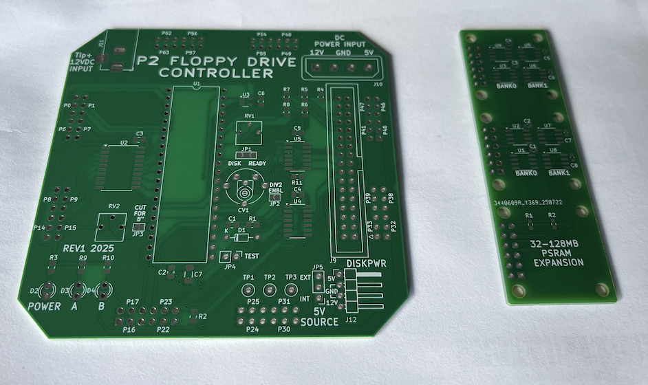
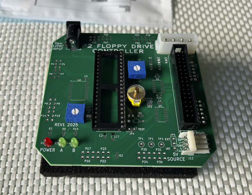
Looking decent. These are my first boards ever done using KiCad and I'm happy that it has worked out so far. I used Eagle before this for all my PCBs and was coupled to it for too long with mental inertia etc, but now I can finally break free and make larger boards with more layers and I'm finding KiCad 9 pretty straightforward to use. Apparently it's much better now and easier to use in later versions vs the earlier ones. I didn't encounter any real dramas using it yet.
Through hole parts I collected seem to fit fine. Just need to solder it all up to test and then write some register access code to try to read floppy sectors etc.
Gee that was quick soldering. Looks the business!...
Nah, just an optical illusion and parts were placed only for checking the fit. Will be soldering it up today though now the paste has warmed up. I want to do the SMD passives & the SOICs on the hotplate first then the through hole stuff.
Board seemed to cook up okay on the hotplate, although I've been deceived before and will need to check with the video microscope.
Well I soldered it up then discovered a (partial) f-up. Thankfully I can recover and still use this board. Turns out my P2-EVAL footprint spacing on my PCB was off by 0.1 inch down one side when I layed it out and my obviously non-thorough double checking efforts didn't find it. Doh!
It's okay though because I don't use these P32-P47 pins for data on my board and in fact it would be good to leave some free breakout groups for USB & video boards to co-exist with this for my Z80 emulator debug etc. I did use two of the pins for the internal 5V supply option (plus a third one from P24-P31), so if the 5V floppy drive current through one single pin header pin exceeds the P2-EVALs 5V supply output in that area it might get warm on that last trace. But I can always use the external Molex supply if that is an issue. So I'm not concerned about it and it's just an annoyance rather than anything too problematic. I just left off the headers for P32-P47 (plus P56-P63) which makes it easier to separate the boards. With all 8 headers fitted it is tight and gets difficult to pull them apart.
Here's the final completely soldered up board. Now need to start testing and coding.