

Flexible P2 BitDAC mode saves the day
 rogloh
Posts: 6,414
rogloh
Posts: 6,414
Here's a nice case where the P2 BitDAC mode shows its flexibility.
I was testing out my parallel RGB LCD panel with the backlight and noticed some corruption when I was using the backlight in PWM mode. This seemed to particularly exacerbate the distortion although it could also be seen to a lesser extent with just full brightness (fixed) LCD backlight on too.
It turned out that due to all the IO pins switching at ~40MHz the ground to the LCD (carried only via two pins of a 40 pin flat flex cable) was bouncing all about. Oscilloscope trace (not posted here) showed all sorts of ugly switching noise on both the ground and parallel LCD signals. The varying backlight power draw also caused power rail noise too. I had guessed I might have signal integrity issues but didn't realize just how bad until I tested it out in this setup.
These parallel video pins were just using normal 3.3V logic mode. I theorized if I enabled bitDAC mode on the parallel RGB pins it could help let me reduce the swing (helping undershoot/overshoot etc) and let the series resistance of the DAC soak up reflections. Turned out this worked a treat! I also reduced the levels by 1 step (DDDDDDDD=%1110_0001).
Here's the bad video before: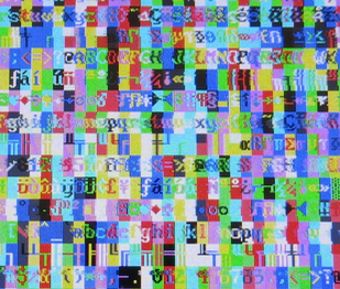
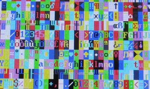
Here's the video after enabling BitDAC mode @3.3V 123.75ohm impedance on the RGB pins (Note 2V @ 75ohms or 3.3V at 990ohms didn't work as nicely). Much better now. ![]() I can also vary the brightness of the LCD backlight smoothly and the text remains sharp.
I can also vary the brightness of the LCD backlight smoothly and the text remains sharp.
Conclusion:
The P2 BitDAC mode can be very useful to tweak output levels if you hit integrity issues in your design.
Comments
That's why some cables have GND on every alternate wire ... or go differential when using dedicated interface chips, aka PHY.
How long is the cable?
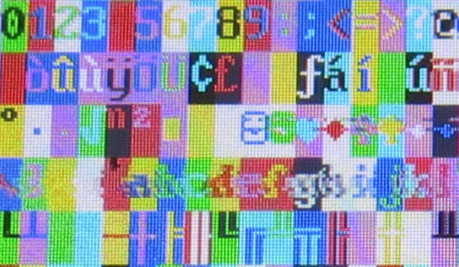
For easier direct viewing, here's a scaled up view of top-right of bad image above:

Using the bitDAC mode to reduce overshoot I guess will have improved drive characteristics irrespective of the cabling.
Yeah I would have preferred that too, unfortunately the design of this LCD module I used only had two grounds and two power lines and 24 RGB plus some other control signals (CLK, DE, SYNCs etc).
The flat flex cable itself is pretty short (~15cm) but there are longer traces on the PCB of the LCD module as well as my own Voyager and P2ME2 boards that contribute to the overall length. Probably a total of 40-50cm I would imagine. Not a lot of care was put into my own parallel RGB layout but it's probably not that bad. I think the shared supply on the LCD module (ie. 5V feeds backlight circuit and then drives a 3.3V LDO for logic power) doesn't isolate the supply well and this contributes to the problem given it is far worse when the backlight is being modulated. I increased the bulk capacitance to 100uF before my own 5V FET power switch feeding the LCD to try to help any voltage sag when the LCD module draws its 1A or so at full backlight power. It did seem to improve things a bit from the original problem I had, but I found using the bitDAC helped a lot more and I am grateful for its flexibility.
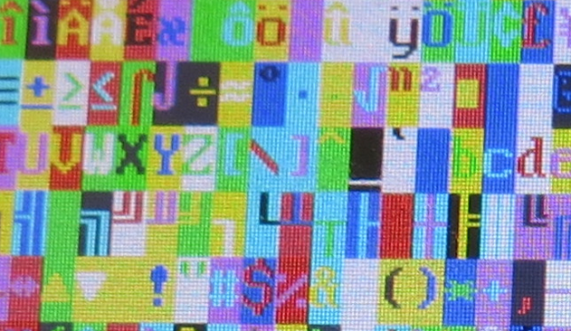
Here's a somewhat clearer comparison at a similar scale from the original larger images.
Bad
Good
That's a great use for that feature.
I think it also might be useful for clock phasing, as you can move a clock signal up or down against a fixed threshold
You can still make everything up to that point have a lot more grounding surface. Like doing flood fills on circuit boards. That would fix it too.
At the top-end of clock frequency - which is the only place we needed such tricks on the HyperRAMs, attenuation wipes out the clock signal altogether. I tried.
Hmm, I guess it wasn't just the top-end, it was anywhere you needed to have a data setup time of a fractional clock cycle. So, although bitDAC can't help with top-end - because the full drive strength is needed then, there is benefit at lower frequencies.
SD cards must be pushing the limits of I/O pins these days. There's no PHY interface chips for doing SD. (EDIT: Or is there?) There'll be tight layout restrictions I imagine though.
Yeah though for that I really need 4 layers. Both my own PCBs are currently just two layers which created some issues for both heat transfer and ground trace area. Despite that, thankfully I've been able to work around it to date.
The idea of hand soldering everything again with a 4 layer respun board is a real turn off right now for me (plus I can't get all the parts) but in any respin one thing I think I'd do is to try thicker copper as well. During its development I've already caused three broken 6 mil tracks on this 2 layer board (unfortunately under a QFP footprint) just with the pressure of a 2x3 pin AVR ISP header connector being attached and removed several times and I have needed some blue wires to fix it. I do try to not press too hard so I think the copper on my PCB must be really thin and can crack easily around the micro-vias or something.
Sounds a tad hairy. Glad you've got it working.
So that's like a series termination. Sounds like that would help reduce slew and thus bounce.
Does that have any current cost, or does the DAC have low ICC when operating right at the rails ?
Yes it should. The ground bounce/noise was lessened on the scope.
Next time I hook up to an ammeter I will compare total system current with/without DAC use. I hope it wouldn't cost too much power although there are a total of 18 RGB data pins using the DACs. I've actually changed the DAC range to be DDDDDDDD=%1100_0011 now so it doesn't go all the way to the rails at either end.
@jmg
Yes you were correct, it does draw a little bit more current in bitDAC mode when I tested it. Here is the total system current from the supply feeding my board:
Meter variation was about 1mA so it was a very stable reading in both tests. Same text mode video output application was tested, only the pin mode varied on the 18 RGB data pins.
Difference was about 28mA @ 12V or 336mW when the DAC was used (it will be slightly less than this at the P2 due to some switching regulator inefficiencies, maybe ~90%). P2 is operating @ 320MHz in this test and the pixel clock @ 40MHz.
I think a resistor string DAC ( 123.75ohm Zo) will draw highest current at 50%, of ~ 13mA per pin, and proportionally less at nearer the rails, so 7/8 is 3.3mA/pin ?
If the swing is pulled too far from GND or VCC, there would also be CMOS threshold effects inside the LCD buffers.
Also tried the following levels:
450 and 422 wrong way round?
Ooops, yes, the higher current case was the DAC mode. Measured it right, but typed in wrong. Must be getting old. I fixed it in the post above. Cheers.
Current increases as voltage levels decrease. Is there a maximum after which current decreases?
Also wondering for 2V output, say, is there a difference in terms of current consumption between %1111_0110 (~3.3V,1.3V) and %1001_0000 (~2V,0V) ?
JMG will be correct, VIO / 2 = 1.65 Volts will be maximum quiescent current draw. Roger's measurements is around 8 mA inc/dec per 1/15 step in 124 ohm mode. (Across how many pins I dunno. Also dunno if that includes active data)
It was only applied across 18 RGB data pins (test snippet below). Yes it included active data being driven (static random text screen).
    repeat x from 0 to 23
        if x==0 or x==1 or x==8 or x==9 or x==16 or x==17
            next
        wrpin(x, %10110_1101_0010_10_00000_0)
Note: this was measured only at the supply voltage of 12V so there will be some current increase in the switchers as the voltage drops.
I might try it later. Am messing with the SPI flash at the moment to try to get the P2 to boot from flash. Not sure why it's not working with the loadp2 instructions and P2ES_flashloader.spin2 etc. Need to check if it is failing the flash programming or failing flash boot. Any useful flash dump code lying about?
EDIT: just found JohnnyMac's flash reader Quick Byte which should let me dump the flash by the looks of it.
Well there's your problem...