

where does the DAC data come from?
 ManAtWork
Posts: 2,369
ManAtWork
Posts: 2,369
I'm struggeling with the documentation, again. There is this block schematic: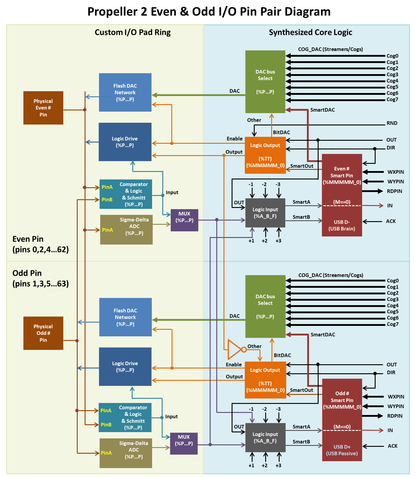
But I can't really find out how the "DAC bus select" works. From reading the silicon doc and examining several software examples, I think I've found out at least some hints:
- There are smart pin DAC modes and non-smart DAC modes
- For smart pin modes the DAC value (16 bits) is determined by the Y register of the smart pin
- for non-smart modes the DAC value (8 bits) is given in the M[7..0] bits of the pin mode if the TT bits are zero
- if TT == P_CHANNEL (%01) then M[3..0] selects the number of the cog or streamer as source
Are the above assumtions correct? And what is BITDAC?
Comments
Next question:
For my QPSK project I need some sort of analogue bus where a sender and a receiver is connected to the same line. When the sender is inactive the DACs remain active to make a resistive termination but they should output a fixed center voltage level ($80) so that no power is wasted and no DC voltage is on the bus.
What happens if the streamer is stopped at the end of a transmission? Does the last DAC output value remain active or is it set to zero? Do I have to change the pin mode (M=10111_10000000, T=00 and S=00000) to output the idle/center level?
I know, I could simply try it out. But I think I'm not the only one who thinks the documentation needs to be improved. Interesting things are possible if we fully understand the features of the smart pin logic (see SAR ADC thread). So I'd really like to understand all of it instead of randomly trying out.
The DAC data can also come from the Streamer or the SETDACS instruction.
BITDAC alows to define two DAC levels for Low and High output. So you can for example drive 1.8 V or 2.5V logic levels.
Ah, thanks, this is exactly what I've been looking for!
(from the "DACs" section in the "COGS" chapter...)
So it wasn't the problem that it's not described in the docs. I just haven't found it because everything is magically connected to each other inside the P2. This is technically ingenious but makes it difficult to document everything you need for a certain topic in just one place. Instead, all the information is scattered over the whole document. You need to read it all or make clever use of the search function.
This is also an interesting feature. But it's very difficult to guess it's purpose and how it works if you don't already know it.
Streamer always stays on the last value if it runs out (either by buffer underrun or by issuing an immediate command that doesn't contain enough data to fill the length of the command)
That diagram needs the 8-bit DAC bus extended down to the comparator too. I do have an ASCII art with that arrangement but at the time I was still half thinking the flash-DAC had an analogue path to the comparator, which it doesn't. Each comparator has its very own dedicated DAC.
In hindsight, probably the main reason I stumbled on this part was there wasn't any indication of being able to use the comparator's DAC beyond a single mode. I now understand the reason is that the 32 bits in WRPIN's mode word isn't enough bits to fully utilise what's possible with the M field. So there is quite a number of removed combinations. The %TT field in particular needs more bits to allow the selecting of data paths without being dependant on the %SSSSS smartpin mode number.
Oh, and the field naming has changed too. M field is now S field. P field is now M field. Job for Rayman.
Ok, I can confirm that it works as expected. I can set the background or idle level with the SETDACS command. The DACs output this value whenever the streamer is not active, i.e. before it was started first and after being stopped with XSTOP. I haven't tested what happens when a run out occurs.
I tried to find anything about BITDAC and found only this:
'BIT_DAC' outputs {2{M[7:4]}} for 'high' or {2{M[3:0]}} for 'low' in DAC_MODEwhich I don't understand. What this {2{ means?
Edit: and how to set it up? Simply WRPIN?
In DAC_MODE, BIT_DAC outputs same 4-bit value in high and low nibbles, i.e. {M[7:4],M[7:4]} for 'high' or {M[3:0],M[3:0]} for 'low'.
The text in the silicon doc just below that line is more useful:
for smart pin mode off (%%SSSSS = %00000): DIR enables output for non-DAC_MODE: 0x = OUT drives output 1x = OTHER drives output for DAC_MODE: 00 = OUT enables ADC, M[7:0] sets DAC level 01 = OUT enables ADC, M[3:0] selects cog DAC channel (COG_DAC mode) 10 = OUT drives BIT_DAC 11 = OTHER drives BIT_DAC for all smart pin modes (%SSSSS > %00000): x0 = output disabled, regardless of DIR x1 = output enabled, regardless of DIR for DAC smart pin modes (%SSSSS = %00001..%00011): 0x = OUT enables ADC in DAC_MODE, M[7:0] overriden 1x = OTHER enables ADC in DAC_MODE, M[7:0] overriden for non-DAC smart pin modes (%SSSSS = %00100..%11111): 0x = SMART/OUT drives output or BIT_DAC if DAC_MODE 1x = SMART/OTHER drives output or BIT_DAC if DAC_MODEOh, yeah, as Tony describes, that's the basic 4-bit to 8-bit depth up-scaling. I must admit it's not easy to read. Tony's arrangement of doubling is easier.
And, yes, setup is done in M field of WRPIN with the above requirements. Which depends on whether you're using the smartpin or not.
Lol, I just realised what the problem with the new fields naming of WRPIN is. It used to be:
%AAAA_BBBB_FFF_PPPPPPPPPPPPP_TT_MMMMM_0But is now:
%AAAA_BBBB_FFF_MMMMMMMMMMMMM_TT_SSSSS_0The change was partly to align with the design schematics, which had used M for its low-level pin modes. But also to avoid any confusion with P also being used for I/O pin reference.
Problem now is instructions use S name for the "source" operand.