

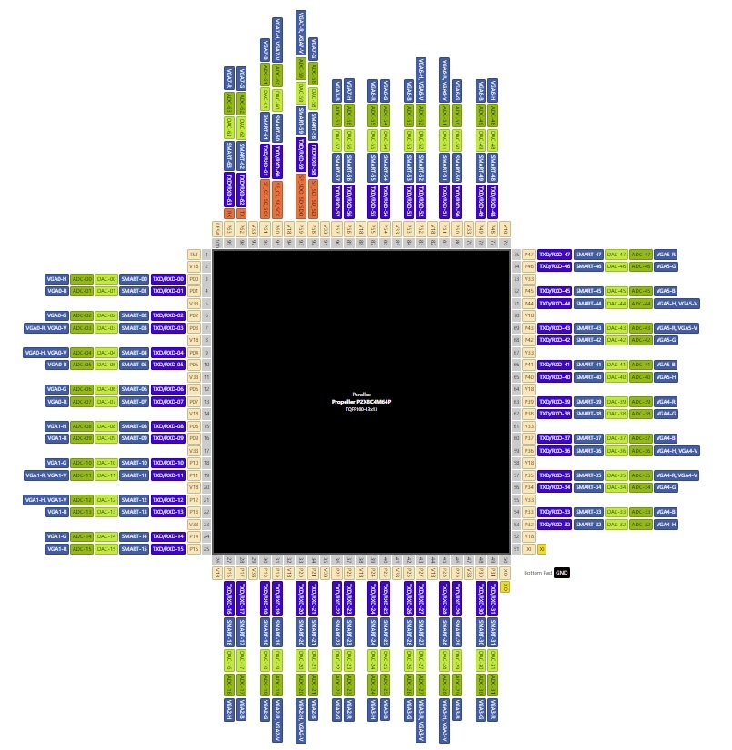
P2 Pinout Diagram
 Cluso99
Posts: 18,071
Cluso99
Posts: 18,071
I sent the json pinout info to Christian and he has now added it to his website here
https://christianflach.de/ic-pinout-diagram-generator/
You will need to scroll down (currently at the end) to find it.
It has only just been posted and there may be errors - I see SF & SD CS & CLK are in error.
Comments
That's very good. The detailed order of special functions like VGA pins is a nice touch. There's many more possibilities though. From the DAC groups that VGA is built on, to DVI/HDMI and parallel buses like HyperBus, OctalSPI and even QuadSPI. Streamer ops (assuming a streamer is used) dictate the pin group ordering of all those. And USB has it's odd/even partnering.
And I forgot PWM too. I’ll add it in when I get a chance.
I was trying to show the flexibility of what can be done with a P2")
We really do have all these peripheral flexibilities with just a little software support. As I described to someone recently, we can do any mix of serial up to 64 pins, so any mix of TXD and RXD pins up to a total of 64 pins, and with any amount of buffering per pin limited only by common (hub) memory of 512KB.
Seems really good!
Until now, I knew nothing about Christian Flach's work.
Time to become one regular follower of his website.
Thanks for posting, Ray!
Updated
https://christianflach.de/ic-pinout-diagram-generator/