

Trying to Figure out SPI lines on P2
 Duane Degn
Posts: 10,588
Duane Degn
Posts: 10,588
in Propeller 2
I'm working on a board which will use the P2, flash and SD card. I figured copying the schematic from the demo board would be a good place to start.
I just noticed the clock lines of the flash and SD card are not controlled by the same pin.
It appears that there's a reason for this but I haven't managed to make sense of this yet.
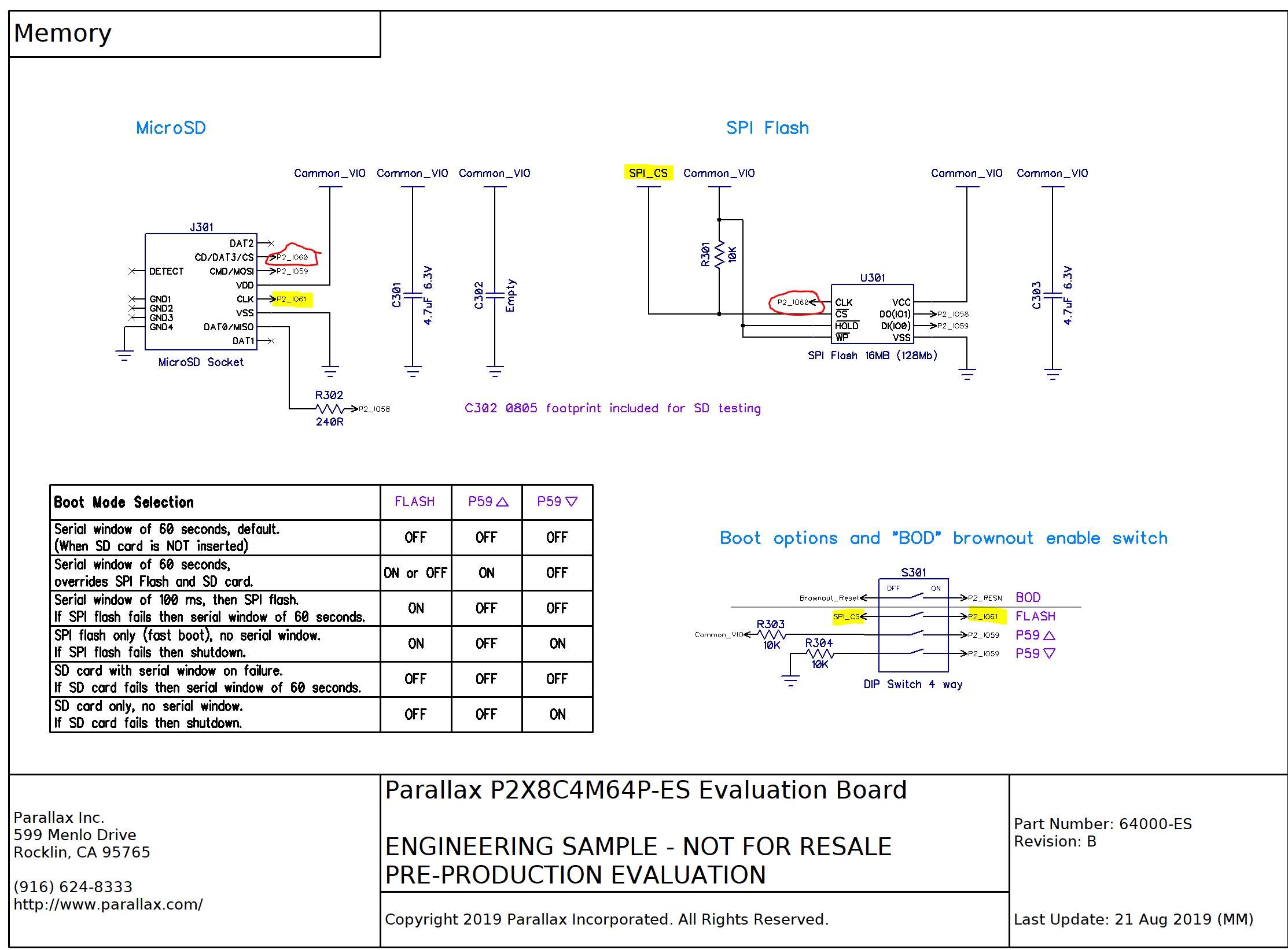
Am I correct in thinking the flash and SD card will have different Clock and chip select lines than one would expect when using multiple SPI devices?
I've tried searching the forum for these answers but I got lost in the pages of results which appear to discuss possible pin combinations.
I just noticed the clock lines of the flash and SD card are not controlled by the same pin.
It appears that there's a reason for this but I haven't managed to make sense of this yet.
Am I correct in thinking the flash and SD card will have different Clock and chip select lines than one would expect when using multiple SPI devices?
I've tried searching the forum for these answers but I got lost in the pages of results which appear to discuss possible pin combinations.
Comments
There are other combinations that are tolerated by the passive device, and P2 does not care which pin the clock is. The boot ROM manages all this via the tables above, as it searches for fitted devices.
In a similar way, sometimes i2c bus designs swap SCL and SDA to give a second set of phantom address / devices.
Rather than use up another I/O line I was able to confirm that the SD card could be connected to the same lines with CLK and CS swapped and co-exist with a Flash device. There was one small problem though in that SD cards are not totally SPI compatible in that when the CS is released the MISO data line "might" and usually do not float. Some do, some don't. This is not a problem during boot but only if you want to use Flash after using SD. The solution was to make sure that the Flash could still drive the line by inserting a series resistor in the SD's Data Out (MISO).
BTW, I further dedicate P57 and P56 for an I2C bus on the P2D2 rather than taking my chances trying to mix that with the already mixed SPI lines
I've included a schematic and note that the RESn line requires a pull-up since P2 does not have any internal pull-up. However the latest version of P2D2 has a pull-down to allow for a RUN instead.
It is important that this detail is captured somewhere in the P2 documentation. This resistor is one of those little things that could cause a problem for people who don't realize it is required in order to reliably use both SPI Flash and SD together with the P2. I don't think it is currently covered anywhere apart from being mentioned once or twice in the forums. New users and anyone else who has forgotten about it may not automatically include this and then stumble into a problem when reading Flash after SD. They'd then have no idea why things stop working without debugging HW, so it really needs to be included somewhere in the document, probably in the Boot Process section which apparently needed more editing anyway according to its title.
It would be good however if that document or somewhere had links to contributed documentation.
btw, while it has been proven that software sequences can convince the SD card to release its data out signal, this is not always guaranteed either, hence the simple just-in-case resistor hack.
@"Duane Degn" - If you (and anyone else) are including USB serial, please consider using the EFM8UB3 chip in QFN20 or QSOP24 packages for this instead of the usual and limited FT232 chips. The bonus is that it can give you a clean RUN reset signal if you use a pull-down on the RESn line and it can automatically disable SD and Flash boot when loading the P2 serially. Also it ignores DTR transitions that aren't load pulses and also adds a smart reset button feature as well as brown-out (and "brown-in") if you use a pull-down for RESn which forces the P2 into reset unless there is a valid RUN signal. You can load the firmware via the USB serial with a simple loader from the PC.
This chip has been tested to work reliably up to 8Mbd in TAQOZ which has proven to be a more punishing test than any of the more predictable echo tests.
If you interface to it via I2C (I use P57 and P56) then besides the 1.8V monitoring that I use, I'm also adding a 'EEPROM" feature to it for non-volatile and persistent data apart from Flash and SD. There's a 128-bit UUID that's also usable.
I can't say it's all clear to me yet but your replies have certainly helped.
Thanks for the suggestion to use the EFM8UB3 chips. I'll look into this possibility.