

Parallax P2 Eval Board
 cgracey
Posts: 14,323
cgracey
Posts: 14,323
This is not completely done, but here's what it looks like. We will build 100 of these with the Amkor-packaged chips.
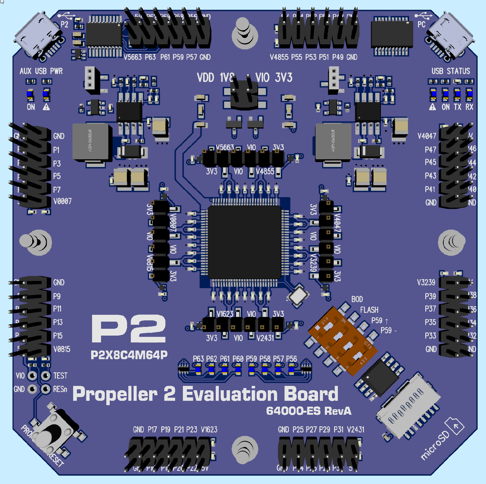
1568 x 1559 - 308K
Comments
Oh, now it's the waiting game... tap, tap, tap... Thanks Chip, and Parallax!
Super itchy to get on the "sign-up sheet".... suuuuper itchy....
j
Purple solder mask would be good.
Don't 'spose you could put a 16MB RAM chip on their too, so we can use this for bootstrapping some stuff (compilers, overlays, frame buffers, etc).
I've been using keyed IDC headers for things like this lately. Saves me from having to think about doing it backwards...
The caps beside the header would interfere with that.
But, this can work if I'm careful...
Having the connectors on the edge makes that easier...
Might have to shape the board to clear ground post if want to use two headers..
Is using other than 3.3 V really a viable options?
eg USB connectors appear to both have FTDI parts ? - so none wire direct to P2 - yet P2-USB testing will surely be quite important ?
Also missing is a HDMI connector ?
A board this size, has a ton of room.
However, I can see somethings have got lost, and some risky moves ...
* P2D2 has options for Crystal and oscillator, and Clipped Sine Oscillators. That is very easy to allow, yet here it is missing ?
I would suggest supplying these boards with a high stability Oscillator fitted, to show off P2 features. (That means Clipped Sine)
Also note P2D2 was improved to have a multi-footprint Oscillator, to cover the range of common osc sizes.
* 5V on all the IO headers ?! - one slip and that's a dead P2!! *POOF* I'd call that far too risky, on limited supply Engineering Samples.
Other comments:
Switching regulators look to still use Schottky diodes, and have a BOM of 23 parts, for each one. Result is a large PCB footprint.
Surely a more compact/ lower BOM solution can be found, so as to not scare customers away with the complexity to merely power a P2 ?
It does not need to be an inductor-included switcher like on P2D2, as those are more expensive, and tend to place size ahead of efficiency.
What package is used for the flash ? - it appears to be TSSOP8, but that is a rare package in Flash.
Usual Candidates would be SO8 (big, but universal) and moving to DFN, and DFN2x3 seems to be a sweet spot, now available 4M/8M/16M sizes.
The DFN2x3 can route quite snugly, right next to a P2 TQFP, see the attached file.
Suggestion: Allow for both DFN2x3 and SO8 flash packages. Even if you never fit the 2x3 package, having it there shows what is possible.
The DFN2x3 helps keep the 'applied footprint' small for P2, which will be important for winning sales.
IIRC Chip tested VIO down to just above 2V, but I think those VIO power options are more for Lower noise Power islands, for Analog work.
Like to use my pin jumper wire and not worry about shorting something.
Mike
I think there's possibly a couple of 3v3 options selected by jumper - a local LDO regulator vs the switcher
That header can also be used to measure local current, or apply a non 3v3 voltage
You mean the boxed headers ?
Moving the caps, to allow a boxed header should be very easy to do.
The pin labels on the inner headers are very confusing in their placement.
ie do they tag the solder pad along side them, or the pin hovering above them ?
Most PCB labels are solder-pad related, and tag the nearest part.
Can those labels be moved, to avoid this ambiguity - eg if they place outside the solder pad, they tag the pad, and pin.
I wonder, is that regulator stable, with no load cap ?
They do not look that easy to replace / change ?
Parallax has a bunch of jumper wires available:
https://www.parallax.com/search?search_api_views_fulltext=Jumper+Wires
The load caps are at the pins - every supply pin has one
.. provided they are connected.
It looks to me like the jumper option, isolates the IO pins from the local regulator, giving it no load C at all ?
I'm really looking forward to getting my hands on one of these!
We could put female sockets, instead of male headers, no problem. we've gone back and forth on that issue.
I hate the size of shrouded connectors, but they would inhibit 5 volt mistakes.
I want one
-Phil
We will install a 16MB chip there with DDR mode. They are $1.25 in volume. Digi-Key has 100k+ in stock.
Those jumpers can also be opened up for current measurements, from either the main VIO supply, which is adjustable, or the local 3.3V regulator.
The main 1.8V and 3.3V switching regulators are both adjustable, up and down. the top two jumpers can also be removed for current measurements on either main supply.
Yes, all of the 2x6 headers are on the same 0.100" grid.
We will put some holes on it.