

Z80 IC - Cluso's take on a new design using modern ICs'
 Cluso99
Posts: 18,069
Cluso99
Posts: 18,069
Stuck at home like many around the world, and pondering what to do in my spare time?
Well, apart from P2 (having a little downtime ATM), I thought I would have another try at designing my take on the venerable Z80 IC. Now. this is the actual Z80 silicon I am referring to. Of course it's been emulated before - even on the P1 (see ZiCog and RamBlade running CPM2.2), and on FPGA's too. Other simpler micros have been re-designed using transistors, gates, and even EEPROMs and RAMs.
This time I plan to use a mix of modern chips, but not an FPGA. I also want to see how fast I can make it run too. Also, I want to minimise where possible, the different types of ICs used.
Thanks to a guy called Ken Shirriff and a group known as Visual 6502, many parts of the Z80 die have been reverse engineered. This gives us a big boost as to how the Z80 works.
righto.com/2014/10/how-z80s-registers-are-implemented-down.html
There is also a silicon gate discussion, and an FPGA implementation, by Goran Devic (Baltazar Studios)
https://baltazarstudios.com/anatomy-z80-gate/
So here we go...
For the register set I intend using the 74LVC646A - Octal bus transceivers and registers with tri-state outputs. This chip is basically a 74LVC245 bus transceiver, and a pair of 74LVC573's all in one 24pin chip. I can use these chips as the bus isolation/transceivers. I can also use these chips as a pair of registers (eg PC, SP, HL etc). One chip will perform the H and H' registers and another the L and L' registers, and so on. An alternative is to use 74LVX245 and 74LVX573 since these use much less power than the standard 74LVC245 and 74LVC573.
For the Incrementer/Decrementer I intend using a parallel FLASH chip(s). Currently I am thinking of something like the SST39VF1602 which is 1Mx16 Flash, but also on the list is the SST39LF040 which is a 512Kx8 Flash. The actual chip used will depend on what Flash chip I use for the main ALU. I will also need another Flash chip to do the "Count 1" gating which checks for A0=L and A1-15=H. While I could use gates, a Flash chip suits my desired goals.
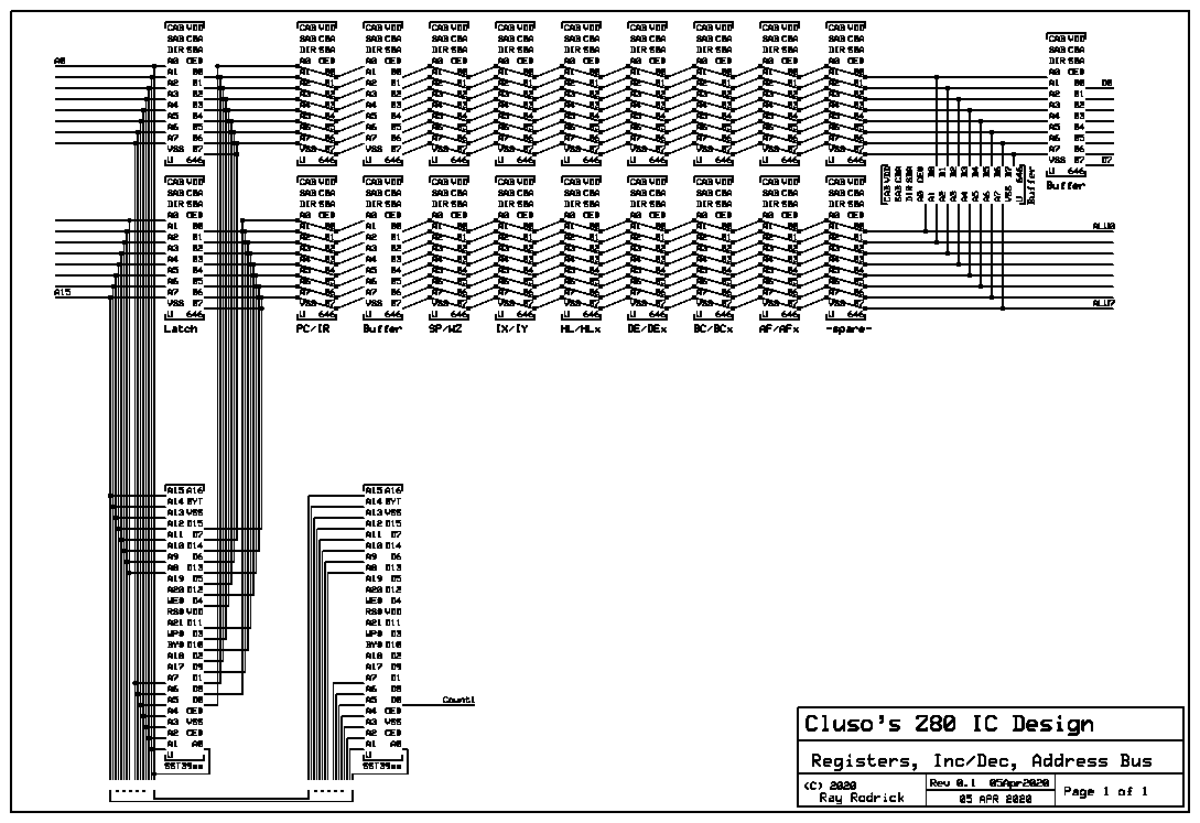
So, without further delay, here is my initial pass on the Z80 internal register set including the PC and SP, the incrementer/decrementer circuit, and the address bus.
Next, I need to add the decode lines for the registers read and write, and the bus and latch enables and directions.
Then I can move on to the ALU implementation which will include the State Controller and Decoder, Oscillator and Single-Stepper, and Data Bus interface. Both will be implemented using Flash chips, and perhaps some miscellaneous gates if necessary. I am not sure whether I need an additional FLAGS register in addition to the F and F' registers, and an Instruction Register in addition to the OP1 and OP2 register. You will also see that I am going to cheat and use an 8-bit ALU, not a two pass 4-bit ALU as used in the real Z80. The Z80 ALU is simpler than usual ALUs in that the incrementer/decrementer is done with the Registers in conjunction with the PC etc.
Looking at the schematics above, you will notice that I've drawn the 74LVC646A's and SST39XXX a little differently. This is to allow the schematic to allow the bus lines to flow thru (ie under) the ICs to make the schematic easier to read (IMHO).
For testing, I'll probably use P2(s)") Should get some nice bus diagrams on my 1920x1080 VGA/HDMI 24" monitor(s). Nothing like being able to just wire a VGA connector directly to the P2
Should get some nice bus diagrams on my 1920x1080 VGA/HDMI 24" monitor(s). Nothing like being able to just wire a VGA connector directly to the P2
Well, apart from P2 (having a little downtime ATM), I thought I would have another try at designing my take on the venerable Z80 IC. Now. this is the actual Z80 silicon I am referring to. Of course it's been emulated before - even on the P1 (see ZiCog and RamBlade running CPM2.2), and on FPGA's too. Other simpler micros have been re-designed using transistors, gates, and even EEPROMs and RAMs.
This time I plan to use a mix of modern chips, but not an FPGA. I also want to see how fast I can make it run too. Also, I want to minimise where possible, the different types of ICs used.
Thanks to a guy called Ken Shirriff and a group known as Visual 6502, many parts of the Z80 die have been reverse engineered. This gives us a big boost as to how the Z80 works.
righto.com/2014/10/how-z80s-registers-are-implemented-down.html
There is also a silicon gate discussion, and an FPGA implementation, by Goran Devic (Baltazar Studios)
https://baltazarstudios.com/anatomy-z80-gate/
So here we go...
For the register set I intend using the 74LVC646A - Octal bus transceivers and registers with tri-state outputs. This chip is basically a 74LVC245 bus transceiver, and a pair of 74LVC573's all in one 24pin chip. I can use these chips as the bus isolation/transceivers. I can also use these chips as a pair of registers (eg PC, SP, HL etc). One chip will perform the H and H' registers and another the L and L' registers, and so on. An alternative is to use 74LVX245 and 74LVX573 since these use much less power than the standard 74LVC245 and 74LVC573.
For the Incrementer/Decrementer I intend using a parallel FLASH chip(s). Currently I am thinking of something like the SST39VF1602 which is 1Mx16 Flash, but also on the list is the SST39LF040 which is a 512Kx8 Flash. The actual chip used will depend on what Flash chip I use for the main ALU. I will also need another Flash chip to do the "Count 1" gating which checks for A0=L and A1-15=H. While I could use gates, a Flash chip suits my desired goals.
So, without further delay, here is my initial pass on the Z80 internal register set including the PC and SP, the incrementer/decrementer circuit, and the address bus.
Next, I need to add the decode lines for the registers read and write, and the bus and latch enables and directions.
Then I can move on to the ALU implementation which will include the State Controller and Decoder, Oscillator and Single-Stepper, and Data Bus interface. Both will be implemented using Flash chips, and perhaps some miscellaneous gates if necessary. I am not sure whether I need an additional FLAGS register in addition to the F and F' registers, and an Instruction Register in addition to the OP1 and OP2 register. You will also see that I am going to cheat and use an 8-bit ALU, not a two pass 4-bit ALU as used in the real Z80. The Z80 ALU is simpler than usual ALUs in that the incrementer/decrementer is done with the Registers in conjunction with the PC etc.
Looking at the schematics above, you will notice that I've drawn the 74LVC646A's and SST39XXX a little differently. This is to allow the schematic to allow the bus lines to flow thru (ie under) the ICs to make the schematic easier to read (IMHO).
For testing, I'll probably use P2(s)
Comments
Personally, I think a more interesting project would be to use the P2 to make a clone of the Z80, both in software and hardware. A single cog can do a complete software emulation (with perfect instruction timing if desired) using XBYTE and no hub RAM, but here I'm talking about implementing all the bus and control signals as well using P2 pins. This would show how well the P2 could replace FPGAs.
Cluso does have an interesting project here, though; it's always interesting to see what you can do turning non-CPU's into CPUs. Do you have any idea how many IC's it will ultimately require?
Thanks for that link. I hadn't seen this although I haven't finished my research into how the decode and state section works yet.
And yes. I finished coding the Z80 emulation of P2 using xbyte last August while visiting my daughter in the UK. I was in the process of testing the instructions. There are test programs to test out the instructions and these fail but because they only test a large number of instructions and making a hash of the results and flags I could not determine where the errors were.
To take the next step I need the FAT driver working to my SD card CPM files. To this end, I have been waiting for Spin2 to settle to recompile the spin1 FAT driver (by Kye) for P2. I've done the P2 ASM driver. But to my horror, spin2 is nothing like spin1, and I fear it will take me ages to go thru Kyes spin and convert to spin2 which has killed my P2 interest for now.
How many ICs?
The Z80 has these register pairs (H & L bytes):
AF, BC, DE, HL, IX, IY, PC, IR. In addition to these AF, BC, DE & HL are duplicates for their alternates. So that makes 14 pairs. Each 74LVC646A can make 2 registers.
The register set (drawn above) requires 14 74LVC646A chips, the address latch requires another 2, the buffers to the address/PC section require 2 more, the data end requires probably 2 plus 1 to join the hi and lo 8-bit data bus.
Add in the Flash chips to perform the Increment/Decrement and Count=1, so another 2 or 3 (8-bit or 16-bit Flash).
This makes 23-24 chips.
Now, I have contemplated an alternative to the above by replacing all the registers, or the two groups, with SRAM. The downside is that the Z80 can transfer directly between registers (eg between HL and BC) and by using SRAM an intermediate latch is required. Also, the inc/dec cannot be done in the same cycle as a register access. Of course, this is a serious reduction in chips!
Next is the ALU which includes the decoder and state machine...
There are 2 74LVC646A chips for OP1 & OP2 latches, 2 or 1 FLASH chips for the ALU (8 or 16 bit),
potentially 1 for the Flags register (not sure if I require this in addition to the main F register), possibly 1 for the IR (instruction register) as input to the 2 or 1 (maybe another 2 or 1 depending on how many state/decodes I need) FLASH chips for the Sequencer/Decoder.
This makes maybe 6-10 chips.
So perhaps 30-36 chips in total, with only 2 types of chips used.
It may be worthwhile to add an optional 64KB (or up to 512KB) SRAM for external memory and maybe another FLASH chip for the external Boot code.
I have been thinking a separate pcb for the register set etc, and a separate pcb for the ALU etc. Maybe these plug into a pcb which contains the external SRAM and FLASH, and space for I/O.
I would be using SMT chips, so the Flash chips would be on tiny plugin pcbs so the code within can easily be updated.
The new info in that link is mainly:
1. Previously unknown behaviour for flag bits 3 and 5, in particular for block instructions when interrupted. All flag bits now known for all instructions probably.
2. Bus request followed by reset allows one to see "sub-atomic" register changes that take place within a single instruction, e.g. L changing before H during LD HL,nn. This is possible because a bus request is granted after any machine cycle, not just at the end of an instruction. I think AF are written back to the register file during the opcode fetch of the next instruction, hence internal changes to F and A are not visible. Changes to the internal WZ 16-bit register can be seen, however. WZ[13:0] can be read in a clever way, which was known already, and I added faster read code.
You'll need to implement WZ and use more flip-flops for interrupts.
Rename your sources to .spin and run them thru fastspin. Fastspin will then compile spin(1) code for P2.
Enjoy!
Mike
The WZ registers are included with the SP pair on my schematics above. I missed calling them out in the chip count. Add another 2 74LVC646A.
You will also see I have a spare pair on my schematics just in case.
I realise that the AF registers are written back from the ALU. Currently I am not sure if I need to hold the flags in the ALU as well.
I do want to emulate the flags correctly. These are generated from the ALU FLASH chip so this should be straight forward.
The current plan is to allow the opcode fetch and register results to be done in the same machine cycle but that would change if I decide to go down the simpler path of using SRAM for the registers as then the internal register bus will not be separate from the PC/IR registers.
BTW I am not going for total emulation of the Z80, just the basic implementation. I am not sure if I want to do the total bus emulation or not.
Obviously using an 8-bit ALU will result in some differences, and my state machine and decoding will be different.
I gave that a try months ago and I didn't like what came out the other side, mainly because I couldn't easily see/understand what had been generated.
You see, I require it to stay resident, and callable, in hub between loading other binaries.
I am bitterly disappointed that the P2 has not turned out to my expectations. I expected to be able to use P1 code with fairly simple conversion to P2, but this is definitely not the case. So I am torn between how to achieve the conversion, and none of the solutions are pretty. I have head in the sand syndrome so I'm looking for something else to chew on in the meantime.
A good example is the conversion I did of Harrison Pham's code to drive the ENC28J60 wired ethernet chip. This was a very mature codebase as P1 code goes when I got to it, but working in FastSpin I realized that I didn't need the separate cog to do fast SPI comms with the ENC28J60. I used fairly naive routines written directly in FastSpin, not running in a separate cog, and it is just as fast as the P1 version with its helper cog and much simpler. I easily got UDP working and then realized that using Harrison's code to do TCP would just be a massive waste of time, because it was a giant hack dealing with the limited memory environment of the P1. On P2 with so much more RAM a much more conventional approach could be taken. Even if I could just paste the P1 code into a dev system to compile for P2, it would create a seriously wasteful and crippled product.
I am very excited about P2. My major worry at this point is that without a solidly official language and development platform, no single OBEX-like resource will form for code sharing. And the Propellers are very highly dependent on such code resources which basically do the same thing as helper hardware in other microcontrollers. If I need code to control a particular accelerometer or EEPROM or servos, and the donor wrote it in C but I'm working in Spin or vice-versa, where does that leave us?
I've been playing with a vintage Z80. Attempting to build a simple Z80 based computer on breadboards. A bit more daunting than I'd hoped, but coming along. I was ready to wire in a memory chip but something released the infamous magic smoke. However, said smoke was colorless and odorless and I've no idea "who" bit the dust.
I suspect something in the clock circuit. I could trouble shoot but it's more fun to just build another (different) timer. :-)
Anyway I'll post a picture of "Medusa" later.
Amanda
@msrobots is probably your guy to talk to about that: Mike did some amazing things to use fastspin and Taqoz together. But it's not hard to write a very simple "os" program that will load other programs (in this case from the PC, but doing it from an SD card would follow the same procedure). I've attached the .zip.